1
Æ
FN7049.1
EL2142
Data Sheet
February 11, 2005
Differential Line Receiver
The EL2142 is a very high bandwidth amplifier designed to
extract the difference signal from noisy environments, and is
thus primarily targeted for applications such as receiving
signals from twisted pair lines, or any application where
common mode noise injection is likely to occur.
The EL2142 is stable for a gain of one, and requires two
external resistors to set the voltage gain.
The output common mode level is set by the reference pin
(V
REF
), which has a -3dB bandwidth of over 100MHz.
Generally, this pin is grounded, but it can be tied to any
voltage reference.
The output can deliver a minimum of ±50mA and is short
circuit protected to withstand a temporary overload
condition.
Features
∑ Differential input range ±2.3V
∑ 150MHz 3dB bandwidth
∑ 400V/µs slewrate
∑ ±5V supplies or single supply
∑ 50mA minimum output current
∑ Output swing (100
load) to within 1.5V of supplies
∑ Low power-11mA typical supply current
∑
Pb-free available (RoHS compliant)
Applications
∑ Twisted pair receiver
∑ Differential line receiver
∑ VGA over twisted pair
∑ ADSL/HDSL receiver
∑ Differential to single ended amplification.
∑ Reception of analog signals in a noisy environment.
Pinout
Ordering Information
PART
NUMBER
PACKAGE
TAPE &
REEL
PKG. DWG. #
EL2142CS
8-pin SOIC
-
MDP0027
EL2142CS-T7
8-pin SOIC
7"
MDP0027
EL2142CS-T13
8-pin SOIC
13"
MDP0027
EL2142CSZ
(See Note)
8-pin SOIC
(Pb-free)
-
MDP0027
EL2142CSZ-T7
(See Note)
8-pin SOIC
(Pb-free)
7"
MDP0027
EL2142CSZ-
T13 (See Note)
8-pin SOIC
(Pb-free)
13"
MDP0027
NOTE: Intersil Pb-free products employ special Pb-free material sets;
molding compounds/die attach materials and 100% matte tin plate
termination finish, which are RoHS compliant and compatible with
both SnPb and Pb-free soldering operations. Intersil Pb-free products
are MSL classified at Pb-free peak reflow temperatures that meet or
exceed the Pb-free requirements of IPC/JEDEC J STD-020.
EL2142
(8-PIN SOIC)
TOP VIEW
CAUTION: These devices are sensitive to electrostatic discharge; follow proper IC Handling Procedures.
1-888-INTERSIL or 1-888-352-6832
|
Intersil (and design) is a registered trademark of Intersil Americas Inc.
Copyright Intersil Americas Inc. 1998, 2005. All Rights Reserved
All other trademarks mentioned are the property of their respective owners.
2
FN7049.1
February 11, 2005
Absolute Maximum Ratings
(T
A
= 25∞C)
Supply Voltage (V
CC
≠V
EE
) . . . . . . . . . . . . . . . . . . . . . . . . . . . 12.6V
Maximum Output Current. . . . . . . . . . . . . . . . . . . . . . . . . . . . ±60mA
Storage Temperature Range . . . . . . . . . . . . . . . . . .-65∞C to +150∞C
Operating Junction Temperature . . . . . . . . . . . . . . . . . . . . . . +150∞C
Recommended Operating Temperature . . . . . . . . . . . -40∞C to 85∞C
CAUTION: Stresses above those listed in "Absolute Maximum Ratings" may cause permanent damage to the device. This is a stress only rating and operation of the
device at these or any other conditions above those indicated in the operational sections of this specification is not implied.
IMPORTANT NOTE: All parameters having Min/Max specifications are guaranteed. Typical values are for information purposes only. Unless otherwise noted, all tests
are at the specified temperature and are pulsed tests, therefore: T
J
= T
C
= T
A
DC Electrical Specifications
V
CC
= +5V, V
EE
= -5V, T
EE
= 25∞C, V
IN
= 0V, R
L
= 100, unless otherwise specified
PARAMETER
DESCRIPTION
MIN
TYP
MAX
UNITS
V
SUPPLY
Supply Operating Range (V
CC
-V
EE
)
±3.0
±5.0
±6.3
V
I
S
Power Supply Current (no load)
11
14
mA
V
OS
Input Referred Offset Voltage
-25
10
40
mV
I
IN
Input Bias Current (V
IN
, V
IN
B, V
REF
)
-20
6
20
µA
Z
IN
Differential Input Resistance
400
k
C
IN
Differential Input Capacitance
1
pF
V
DIFF
Differential Input Range
±2.0
±2.3
V
A
VOL
Open Loop Voltage Gain
75
dB
V
IN
Input Common Mode Voltage Range
-2.6
+4.0
V
V
OUT
Output Voltage Swing (50
load to GND)
±2.9
±3.1
V
I
OUT
(min)
Minimum Output Current
50
60
mA
V
N
Input Referred Voltage Noise
36
nV/
Hz
V
REF
Output Voltage Control Range
-2.5
+3.3
V
PSRR
Power Supply Rejection Ratio
60
70
dB
CMRR2
Input Common Mode Rejection Ratio (V
IN
= ±2V)
60
70
dB
CMRR1
Input Common Mode Rejection Ratio (full V
IN
range)
50
60
dB
AC Electrical Specifications
V
CC
= +5V, V
EE
= -5V, T
A
= 25C, V
IN
= 0V, R
LOAD
= 100, unless otherwise specified
PARAMETER
DESCRIPTION
MIN
TYP
MAX
UNITS
BW(-3dB)
-3dB Bandwidth (Gain =1)
150
MHz
SR
Slewrate
400
V/µs
T
STL
Settling time to 1%
15
ns
GBWP
Gain bandwidth product
200
MHz
V
REF
BW(-3dB)
V
REF
-3dB Bandwidth
130
MHz
V
REF
SR
V
REF
Slewrate
100
V/µsec
dG
Differential gain at 3.58MHz
0.2
%
d
Differential phase at 3.58MHz
0.2
∞
EL2142
3
FN7049.1
February 11, 2005
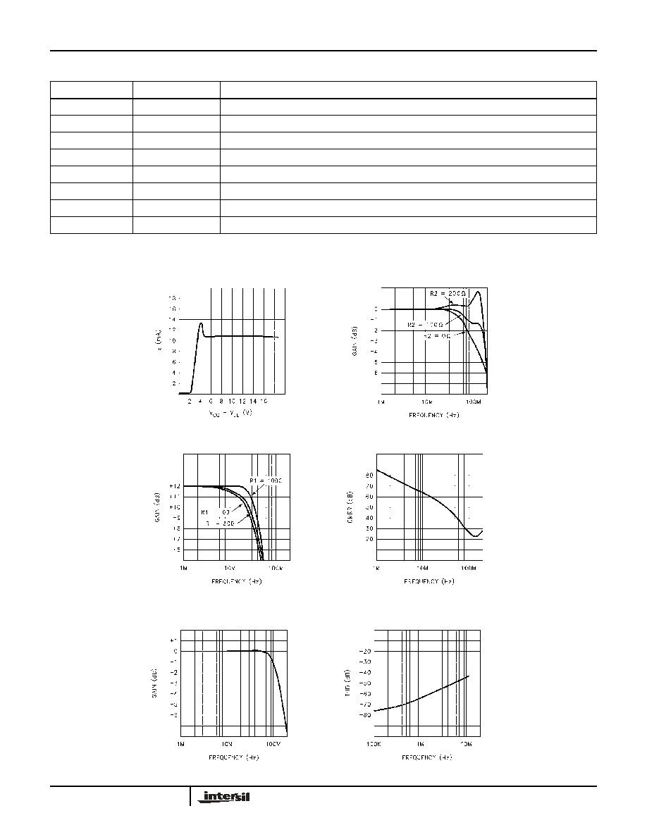
Typical Performance Curves
Pin Descriptions
PIN NUMBER
PIN NAME
FUNCTION
1
V
FB
Feedback input
2
V
IN
Non-inverting input
3
V
INB
Inverting input
4
V
REF
Sets output voltage level to V
REF
when V
IN
=V
INB
5
NC
6
V
CC
Positive supply voltage
7
V
EE
Negative supply voltage
8
V
OUT
Output voltage
Frequency Response
(Gain = 1)
I
S
vs Supply Voltage
Frequency Response
vs Resistor R1 (Gain = 4)
V
REF
Frequency Response
Distortion vs Frequency
(Gain = 3, R
LOAD
= 100
)
V
IN
= 2V
PK-PK
CMRR vs Frequency
EL2142
4
FN7049.1
February 11, 2005
Applications Information
Gain Equation
V
OUT
= ((R2+R1)/R1) x (V
IN
-V
INB
+V
REF
) when R1 tied to
GND
V
OUT
= ((R2+R1)/R1) x (V
IN
-V
INB
) when R1 tied to V
REF
Choice of Feedback Resistor
For a gain of one, V
OUT
may be shorted back to V
FB
, but
100
-200
improves the bandwidth. For gains greater than
one, there is little to be gained from choosing resistor R1
value below 200
, for it would only result in increased power
dissipation and potential signal distortion. Above 200
, the
bandwidth response will develop some peaking (for a gain of
one), but substantially higher R1 values may be used for
higher voltage gains, such as up to 1k
at a gain of four
before peaking will develop.
Capacitance Considerations
As with many high bandwidth amplifiers, the EL2142 prefers
not to drive highly capacitive loads. It is best if the
capacitance on V
OUT
is kept below 10pF if the user does not
want gain peaking to develop. The V
FB
node forms a
potential pole in the feedback loop, so capacitance should be
minimized on this node for maximum bandwidth.
The amount of capacitance tolerated on any of these nodes
in an actual application will also be dependent on the gain
setting and the resistor values in the feedback network.
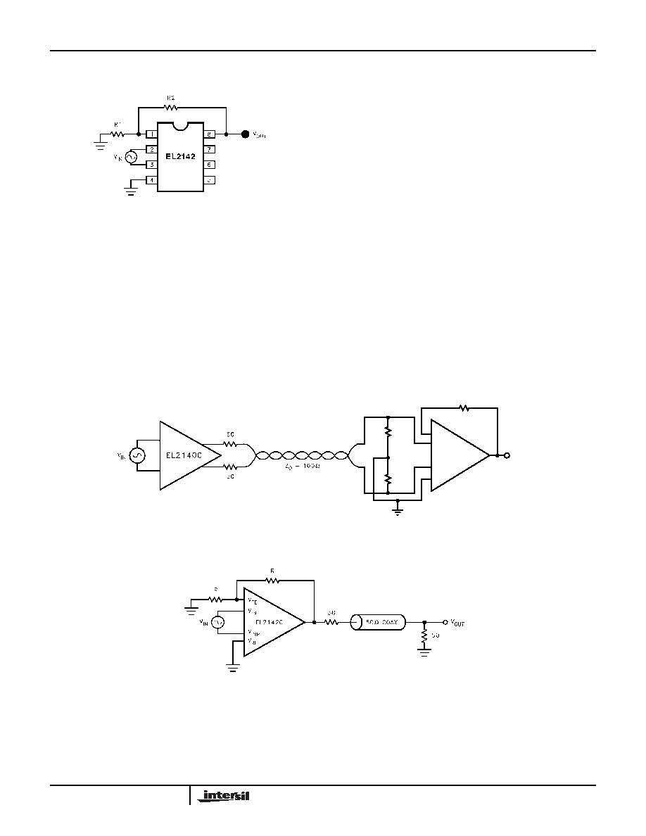
Typical Applications Circuits
FIGURE 1. TYPICAL TWISTED PAIR APPLICATION
50
V
FB
50
EL2142
V
IN
V
INB
V
REF
V
OUT
100
FIGURE 2. COAXIAL CABLE DRIVER PAIR APPLICATION
EL2142
5
FN7049.1
February 11, 2005
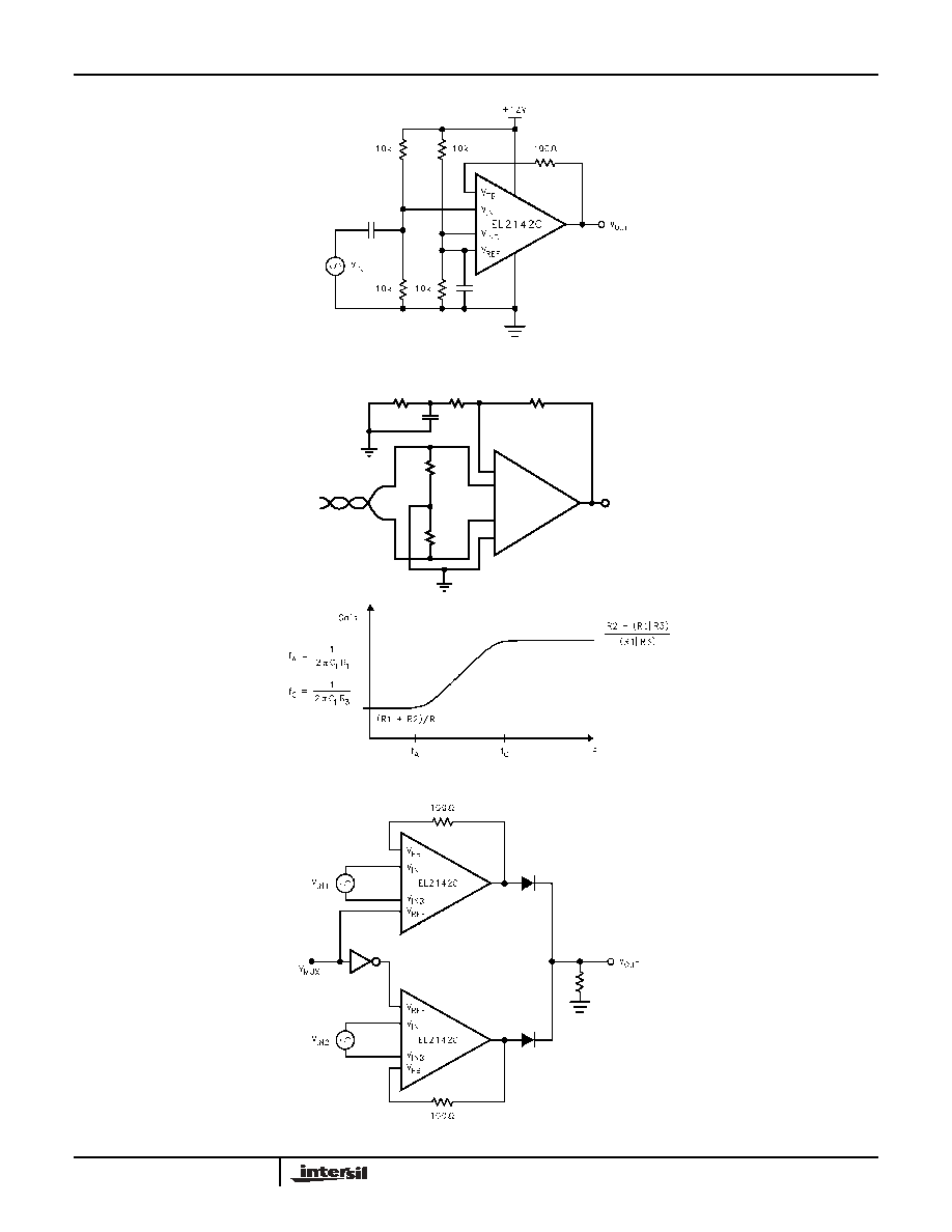
FIGURE 3. SINGLE SUPPLY RECEIVER
FIGURE 4. COMPENSATED LINE RECEIVER
50
V
FB
50
EL2142
V
IN
V
INB
V
REF
V
OUT
R2
R1
R3
C
1
Z
0
= 100
FIGURE 5. TWO CHANNEL MULTIPLEXER
EL2142