 | –≠–ª–µ–∫—Ç—Ä–æ–Ω–Ω—ã–π –∫–æ–º–ø–æ–Ω–µ–Ω—Ç: EL2171CN | –°–∫–∞—á–∞—Ç—å:  PDF PDF  ZIP ZIP |
1
Æ
FN7032
CAUTION: These devices are sensitive to electrostatic discharge; follow proper IC Handling Procedures.
1-888-INTERSIL or 321-724-7143
|
Intersil (and design) is a registered trademark of Intersil Americas Inc.
Copyright © Intersil Americas Inc. 2003. All Rights Reserved. Elantec is a registered trademark of Elantec Semiconductor, Inc.
All other trademarks mentioned are the property of their respective owners.
EL2071, EL2171
150MHz Current Feedback Amplifier
The EL2071 and EL2171 are wide
bandwidth, fast settling monolithic
amplifiers built using an advanced
complementary bipolar process. The EL2071 has a
disable/enable feature which allows power down and analog
multiplexing. These amplifiers use current-mode feedback to
achieve more bandwidth at a given gain than conventional
operational amplifiers. Designed for closed-loop gains of ±7
to ±50, the EL2071 and EL2171 have a 150MHz - 3dB
bandwidth (A
V
= +20), and 2.5ns rise/fall time, while
consuming only 15mA of supply current. The EL2071
consumes only 1.5mA when disabled.
The wide 150MHz bandwidth and extremely linear phase
(0.2dB deviation from linear at 50MHz) allow superior signal
fidelity. These features make the EL2071 and EL2171
especially suited for many digital communication system
applications.
The EL2071's and EL2171's settling to 0.1% in 10ns and
ability to drive capacitive loads make them ideal in flash A/D
applications. D/A systems can also benefit from the EL2071
and EL2171, especially if linearity and drive levels are
important.
Elantec products and facilities comply with MIL-I-45208A,
and other applicable quality specifications. For information
on Elantec's processing, see Elantec document, QRA-1:
Elantec's Processing, Monolithic Integrated Circuits.
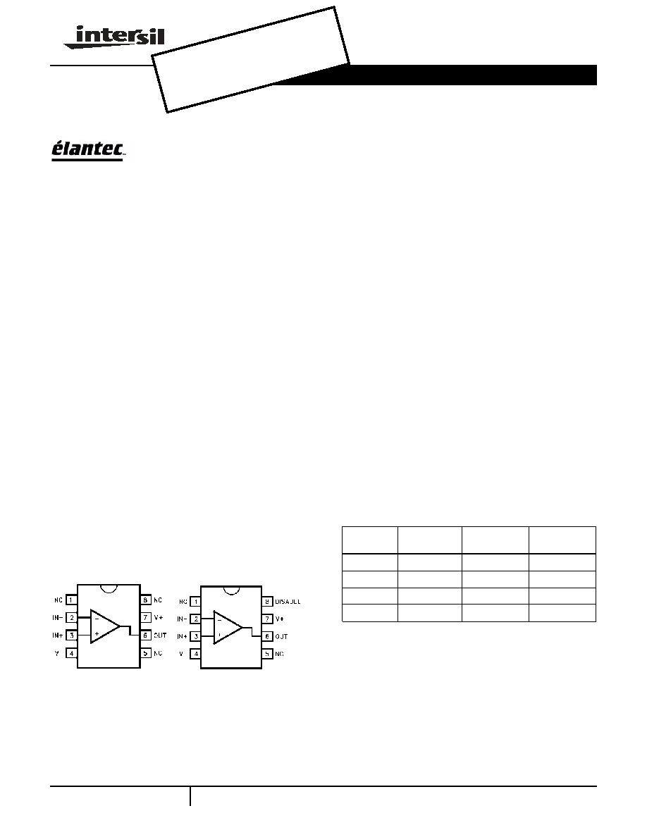
Pinout
Features
∑ 150MHz - 3dB bandwidth, A
V
= 20
∑ 10ns settling to 0.1%
∑ V
S
= ±5V @ 15mA
∑ 2.5ns rise/fall times (2V step)
∑ Overload/short-circuit protected
∑ ±7 to ±50 closed-loop gain range
∑ Low cost
∑ EL2171 is direct replacement for CLC401
∑ Disable capability on EL2071
Applications
∑ Line drivers
∑ DC-coupled log amplifiers
∑ High-speed modems, radios
∑ High-speed A/D conversion
∑ D/A I-V conversion
∑ Photodiode, CCD preamps
∑ IF processors
∑ High-speed communications
∑ Analog multiplexing (using disable--EL2071)
∑ Power down mode (using disable--EL2071)
EL2171
(8-PIN PDIP, SO)
TOP VIEW
Manufactured under U.S. Patent No. 4,893,091
EL2071
(8-PIN PDIP, SO)
TOP VIEW
Ordering Information
PART
NUMBER
TEMP.
RANGE
PACKAGE
PKG. NO.
EL2171CN
-40∞C to +85∞C
8-Pin PDIP
MDP0031
EL2171CS
-40∞C to +85∞C
8-Pin SO
MDP0027
EL2071CN
-40∞C to +85∞C
8-Pin PDIP
MDP0031
EL2071CS
-40∞C to +85∞C
8-Pin SO
MDP0027
Data Sheet
December 1995, Rev. E
OBSO
LETE
PRO
DUCT
NO R
ECOM
MEND
ED R
EPLA
CEME
NT
conta
ct ou
r Tec
hnica
l Sup
port C
enter
at
1-888
-INTE
RSIL
or w
ww.in
tersil
.com
/tsc
2
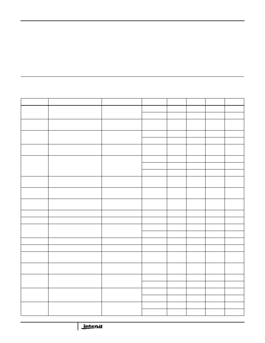
Absolute Maximum Ratings
(T
A
= 25∞C)
Supply Voltage (V
S
) . . . . . . . . . . . . . . . . . . . . . . . . . . . . . . . . . . .±7V
(Output Current Output is short-circuit protected to ground, however,maximum
reliability is obtained if I
OUT
does not exceed 70mA.)
Common Mode Input Voltage . . . . . . . . . . . . . . . . . . . . . . . . . . ±V
S
Differential Input Voltage . . . . . . . . . . . . . . . . . . . . . . . . . . . . . . . .5V
Power Dissipation . . . . . . . . . . . . . . . . . . . . . . . . . . . . . See Curves
Operating Temperature . . . . . . . . . . . . . . . . . . . . . . .-40∞C to +85∞C
Operating Junction Temperature
Ceramic Packages. . . . . . . . . . . . . . . . . . . . . . . . . . . . . . . . . . 175∞C
Plastic Packages . . . . . . . . . . . . . . . . . . . . . . . . . . . . . . . . . . . 150∞C
Storage Temperature . . . . . . . . . . . . . . . . . . . . . . . . -60∞C to +150∞C
CAUTION: Stresses above those listed in "Absolute Maximum Ratings" may cause permanent damage to the device. This is a stress only rating and operation of the
device at these or any other conditions above those indicated in the operational sections of this specification is not implied.
IMPORTANT NOTE: All parameters having Min/Max specifications are guaranteed. Typical values are for information purposes only. Unless otherwise noted, all tests
are at the specified temperature and are pulsed tests, therefore: T
J
= T
C
= T
A
Open-Loop DC Electrical Specifications
V
S
= ±5V, R
L
= 100
, unless otherwise specified
PARAMETER
DESCRIPTION
TEST CONDITIONS
TEMP
MIN
TYP
MAX
UNITS
V
OS
Input Offset Voltage
25∞C
3
6
mV
T
MIN
, T
MAX
10
mV
TC V
OS
Average Offset
Voltage Drift
(Note 1)
All
20
50
µV/∞C
+I
IN
+Input Current
25∞C, T
MAX
10
20
µA
T
MIN
36
µA
TC (+I
IN
)
Average +Input
Current Drift
(Note 1)
All
100
200
nA/∞C
-I
IN
-Input Current
25∞C
10
30
µA
T
MIN
46
µA
T
MAX
40
µA
TC (-I
IN
)
Average -Input
Current Drift
(Note 1)
All
100
200
nA/∞C
PSRR
Power Supply
Rejection Ratio
(Note 2)
All
50
55
dB
CMRR
Common-Mode
Rejection Ratio
All
40
50
dB
I
S
Supply Current--Quiescent
No Load
All
15
21
mA
I
SOFF
Supply Current--Disabled
EL2071 (Note 3)
All
1.5
3.0
mA
+R
IN
+Input Resistance
25∞C, T
MAX
100
200
k
T
MIN
50
k
C
IN
Input Capacitance
All
0.5
2.5
pF
R
OUT
Output Resistance (DC)
All
0.2
0.3
R
OUTD
Output Resistance (DC)
EL2071
Disabled
All
100
200
k
C
OUTD
Output Capacitance (DC)
EL2071
Disabled
All
0.5
2.0
pF
CMIR
Common-Mode Input
Range
(Note 4)
25∞C, T
MAX
±2.5
±2.8
V
T
MIN
±2
V
I
OUT
Output Current
25∞C, T
MAX
50
70
mA
T
MIN
35
mA
V
OUT
Output Voltage Swing
No Load
25∞C, T
MAX
3.2
3.5
V
T
MIN
3
V
EL2071, EL2171
3
V
OUTL
Output Voltage Swing
R
L
= 100
25∞C
3.2
3.4
V
R
OL
Transimpedance
25∞C
250
1000
V/mA
I
LOGIC
Pin 8 Current @+5V
EL2071
All
500
750
µA
V
DIS
Minimum Pin 8
V to Disable
EL2071
25∞C
4.3
T
MIN
4.0
V
T
MAX
4.6
V
EN
Maximum Pin 8
V to Enable
EL2071
All
0.7
V
I
DIS
Minimum Pin 8
I to Disable
EL2071
All
750
µA
I
EN
Maximum Pin 8
I to Enable
EL2071
All
35
µA
NOTES:
1. Measured from T
MIN
to T
MAX
.
2. PSRR is measured at V
S
= ±4.5V and V
S
= ±5.5V. Both supplies are changed simultaneously.
3. Supply current when disabled is measured at the negative supply.
4. Common-Mode Input Range for Rated Performance.
Closed-Loop AC Electrical Specifications
V
S
= ±5V, R
F
= 1.5k
, A
V
= +20, R
L
= 100
unless otherwise specified
PARAMETER
DESCRIPTION
TEST CONDITIONS
TEMP
MIN
TYP
MAX
UNITS
FREQUENCY RESPONSE
SSBW
-3dB Bandwidth
(V
OUT
< 2.0 V
PP
)
25∞C
100
150
MHz
T
MIN
100
MHZ
T
MAX
70
MHz
LSBW
-3dB Bandwidth
(V
OUT
< 5.0 V
PP
)
25∞C, T
MIN
65
100
MHz
T
MAX
55
MHz
GAIN FLATNESS
GFPL
Peaking
V
OUT
< 2.0 V
PP
< 25MHz
25∞C
0.0
0.1
dB
T
MIN
, T
MAX
0.1
dB
GFPH
Peaking
V
OUT
< 2.0 V
PP
> 25MHz
25∞C
0.0
0.2
dB
T
MIN
, T
MAX
0.2
dB
GFR
Rolloff
V
OUT
< 2.0 V
PP
< 50MHz
25∞C
0.2
1.0
dB
T
MIN
1.0
dB
T
MAX
1.3
dB
LPD
Linear Phase Deviation
V
OUT
< 2.0 V
PP
< 50MHz
25∞C, T
MIN
0.2
1.0
∞
T
MAX
1.5
∞
TIME-DOMAIN RESPONSE
t
R1
, t
F1
Rise Time, Fall Time
2.0V Step
25∞C, T
MIN
2.5
3.5
ns
T
MAX
5
ns
t
R2
, t
F2
Rise Time, Fall Time
5.0V Step
25∞C, T
MIN
5
7
ns
T
MAX
8
ns
t
S
Settling Time to 0.1%
2.0V Step
All
10
15
ns
Open-Loop DC Electrical Specifications
V
S
= ±5V, R
L
= 100
, unless otherwise specified (Continued)
PARAMETER
DESCRIPTION
TEST CONDITIONS
TEMP
MIN
TYP
MAX
UNITS
EL2071, EL2171
4
OS
Overshoot
2.0V Step
All
0
10
%
SR
Slew Rate
25∞C, T
MIN
800
1200
V/µs
T
MAX
700
V/µs
DISTORTION
HD2
2nd Harmonic
Distortion @20MHz
2V
PP
25∞C
-45
-35
dBc
T
MIN
, T
MAX
-35
dBc
HD3
3rd Harmonic
Distortion @20MHz
2V
PP
25∞C
-60
-50
dBc
T
MIN
-50
dBc
T
MAX
-45
dBc
EQUIVALENT INPUT NOISE
NF
Noise Floor >100kHz
25∞C
-158
-155
dBm (1Hz)
T
MIN
-155
dBm (1Hz)
T
MAX
-154
dBm (1Hz)
INV
Integrated Noise
100kHz to 200MHz
25∞C
35
50
µV
T
MIN
50
µV
T
MAX
55
µV
DISABLE/ENABLE PERFORMANCE--EL2071C
T
OFF
V
OUT
= 2 V
PP
Disable Time to >40dB
20MHz
All
70
200
ns
T
ON
Enable Time
All
40
100
ns
ISO
Off Isolation
20MHz
All
50
55
dB
Closed-Loop AC Electrical Specifications
V
S
= ±5V, R
F
= 1.5k
, A
V
= +20, R
L
= 100
unless otherwise specified (Continued)
PARAMETER
DESCRIPTION
TEST CONDITIONS
TEMP
MIN
TYP
MAX
UNITS
EL2071, EL2171
5
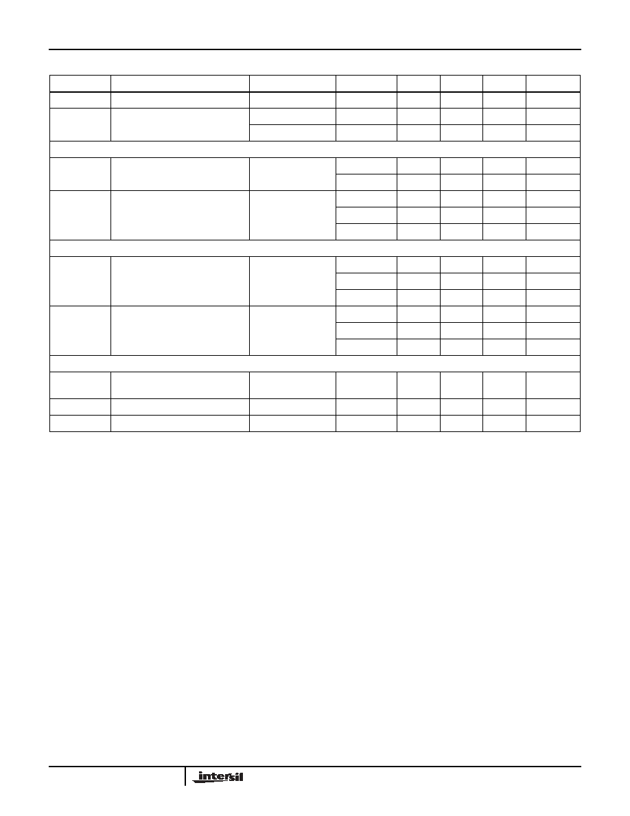
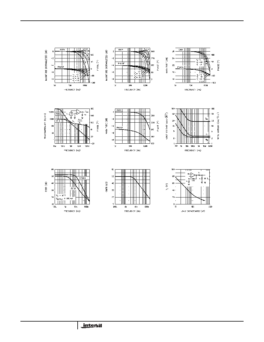
Typical Performance Curves
Non-Inverting
Frequency Response
Inverting Frequency
Response
Frequency Response for
Various R
L
s
Equivalent Input Noise
Frequency Response,
A
V
= -1, R
F
= 2.5k
Single Power Supply
Rejection Ratio
Common Mode
Rejection Ratio (A
V
= +20)
Recommended R
S
vs
Load Capacitance
Open-Loop Transimpedance
Gain and Phase
EL2071, EL2171