 | –≠–ª–µ–∫—Ç—Ä–æ–Ω–Ω—ã–π –∫–æ–º–ø–æ–Ω–µ–Ω—Ç: EL2250CN | –°–∫–∞—á–∞—Ç—å:  PDF PDF  ZIP ZIP |
1
Æ
FN7061.2
CAUTION: These devices are sensitive to electrostatic discharge; follow proper IC Handling Procedures.
1-888-INTERSIL or 321-724-7143
|
Intersil (and design) is a registered trademark of Intersil Americas Inc.
Copyright © Intersil Americas Inc. 2002-2005. All Rights Reserved.
All other trademarks mentioned are the property of their respective owners.
EL2250, EL2450
125MHz Single Supply Dual/Quad Op
Amps
The EL2250/EL2450 are part of a family of the electronics
industries fastest single supply op amps available. Prior
single supply op amps have generally been limited to
bandwidths and slew rates to that of the EL2250/EL2450.
The 125MHz bandwidth, 275V/µs slew rate, and
0.05%/0.05∞ differential gain/differential phase makes this
part ideal for single or dual supply video speed applications.
With its voltage feedback architecture, this amplifier can
accept reactive feedback networks, allowing them to be
used in analog filtering applications. The inputs can sense
signals below the bottom supply rail and as high as 1.2V
below the top rail. Connecting the load resistor to ground
and operating from a single supply, the outputs swing
completely to ground without saturating. The outputs can
also drive to within 1.2V of the top rail. The EL2250/EL2450
will output ±100mA and will operate with single supply
voltages as low as 2.7V, making them ideal for portable, low
power applications.
The EL2250/EL2450 are available in PDIP and SO
packages in industry standard pin outs. Both parts operate
over the industrial temperature range of -40∞C to +85∞C, and
are part of a family of single supply op amps. For single
amplifier applications, see the EL2150/EL2157. For dual and
triple amplifiers with power down and output voltage clamps,
see the EL2257/EL2357.
Features
∑ Specified for +3V, +5V, or ±5V applications
∑ Large input common mode range
0V < V
CM
< V
S
-1.2V
∑ Output swings to ground without saturating
∑ -3dB bandwidth = 125MHz
∑ ±0.1dB bandwidth = 30MHz
∑ Low supply current = 5mA (per amplifier)
∑ Slew rate = 275V/µs
∑ Low offset voltage = 4mV max
∑ Output current = ±100mA
∑ High open loop gain = 80dB
∑ Differential gain = 0.05%
∑ Differential phase = 0.05∞
∑ Pb-free plus anneal available (RoHS compliant)
Applications
∑ Video amplifiers
∑ PCMCIA applications
∑ A/D drivers
∑ Line drivers
∑ Portable computers
∑ High speed communications
∑ RGB printers, FAX, scanners
∑ Broadcast equipment
∑ Active filtering
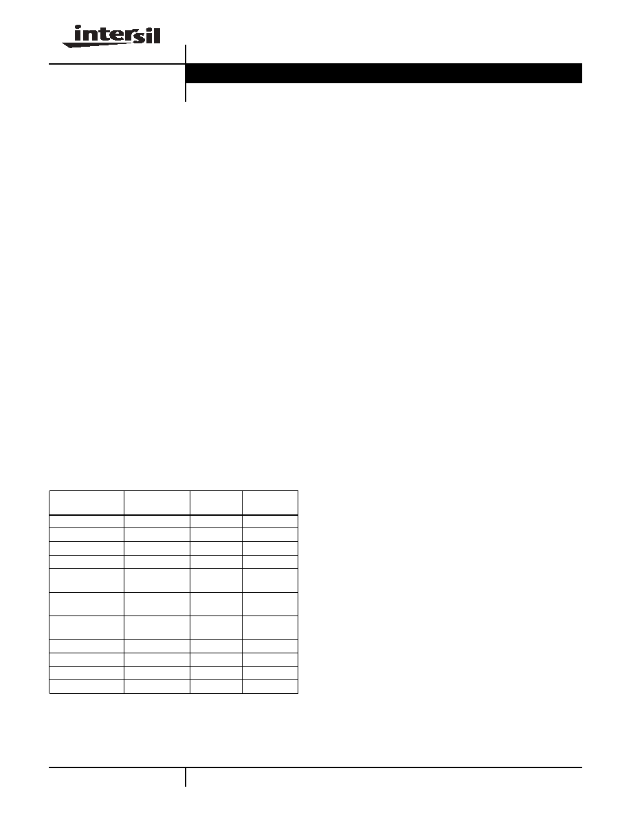
Ordering Information
PART NUMBER
PACKAGE
TAPE &
REEL
PKG. DWG. #
EL2250CN
8-Pin PDIP
-
MDP0031
EL2250CS
8-Pin SO
-
MDP0027
EL2250CS-T7
8-Pin SO
7"
MDP0027
EL2250CS-T13
8-Pin SO
13"
MDP0027
EL2250CSZ
(See Note)
8-Pin SO
(Pb-free)
-
MDP0027
EL2250CSZ-T7
(See Note)
8-Pin SO
(Pb-free)
7"
MDP0027
EL2250CSZ-T13
(See Note)
8-Pin SO
(Pb-free)
13"
MDP0027
EL2450CN
14-Pin PDIP
-
MDP0031
EL2450CS
14-Pin SO
-
MDP0027
EL2450CS-T7
14-Pin SO
7"
MDP0027
EL2450CS-T13
14-Pin SO
13"
MDP0027
NOTE:
Intersil Pb-free plus anneal products employ special Pb-free
material sets; molding compounds/die attach materials and 100%
matte tin plate termination finish, which are RoHS compliant and
compatible with both SnPb and Pb-free soldering operations. Intersil
Pb-free products are MSL classified at Pb-free peak reflow
temperatures that meet or exceed the Pb-free requirements of
IPC/JEDEC J STD-020.
Data Sheet
June 7, 2005

2
FN7061.2
June 7, 2005
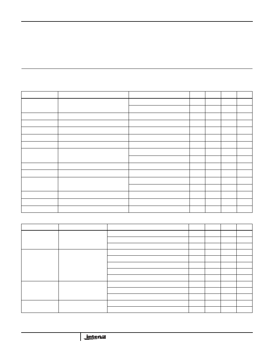
Pinouts
EL2250C
(8-PIN SO, PDIP)
TOP VIEW
EL2450
(14-PIN SO, PDIP)
TOP VIEW
1
2
3
4
8
7
6
5
-
+
-
+
A
B
OUTA
INA-
INA+
GND
VS+
OUTB
INB-
INB+
1
2
3
4
14
13
12
11
5
6
7
10
9
8
OUTA
INA-
INA+
VS+
OUTD
IND-
IND+
GND
INB+
INB-
OUTB
INC+
INC-
OUTC
- +
-
+
- +
-
+
B
C
A
D
EL2250, EL2450
3
FN7061.2
June 7, 2005
Absolute Maximum Ratings
(T
A
= 25∞C)
Supply Voltage between V
S
and GND . . . . . . . . . . . . . . . . . . +12.6V
Input Voltage (IN+, IN-) . . . . . . . . . . . . . . . . . . . GND-0.3V,V
S
+0.3V
Differential Input Voltage . . . . . . . . . . . . . . . . . . . . . . . . . . . . . . .±6V
Maximum Output Current. . . . . . . . . . . . . . . . . . . . . . . . . . . . . 90mA
Output Short Circuit Duration. . . . . . . . . . . . . . . . . . . . . . . . (Note 1)
Power Dissipation . . . . . . . . . . . . . . . . . . . . . . . . . . . . . See Curves
Storage Temperature Range . . . . . . . . . . . . . . . . . .-65∞C to +150∞C
Ambient Operating Temperature Range . . . . . . . . . .-40∞C to +85∞C
Operating Junction Temperature . . . . . . . . . . . . . . . . . . . . . . . 150∞C
CAUTION: Stresses above those listed in "Absolute Maximum Ratings" may cause permanent damage to the device. This is a stress only rating and operation of the
device at these or any other conditions above those indicated in the operational sections of this specification is not implied.
IMPORTANT NOTE: All parameters having Min/Max specifications are guaranteed. Typical values are for information purposes only. Unless otherwise noted, all tests
are at the specified temperature and are pulsed tests, therefore: T
J
= T
C
= T
A
DC Electrical Specifications
V
S
= +5V, GND = 0V, T
A
= 25∞C, V
CM
= 1.5V, V
OUT
= 1.5V, unless otherwise specified.
PARAMETER
DESCRIPTION
TEST CONDITIONS
MIN
TYP
MAX
UNIT
V
OS
Offset Voltage
EL2250
-2
2
mV
EL2450
-4
4
mV
TCV
OS
Offset Voltage Temperature Coefficient
Measured from T
MIN
to T
MAX
10
µV/∞C
IB
Input Bias Current
V
IN
= 0V
-5.5
-10
µA
I
OS
Input Offset Current
V
IN
= 0V
-750
150
750
nA
TCI
OS
Input Bias Current Temperature Coefficient Measured from T
MIN
to T
MAX
50
nA/∞C
PSRR
Power Supply Rejection Ratio
V
S
= +2.7V to +12V
55
70
dB
CMRR
Common Mode Rejection Ratio
VCM = 0V to +3.8V
55
65
dB
VCM = 0V to +3.0V
55
70
dB
CMIR
Common Mode Input Range
0
V
S
-1.2
V
R
IN
Input Resistance
Common Mode
1
2
M
C
IN
Input Capacitance
SO Package
1
pF
PDIP Package
1.5
pF
R
OUT
Output Resistance
A
V
= +1
40
m
I
S
Supply Current (per amplifier)
V
S
= +12V
5
6.5
mA
PSOR
Power Supply Operating Range
2.7
12.0
V
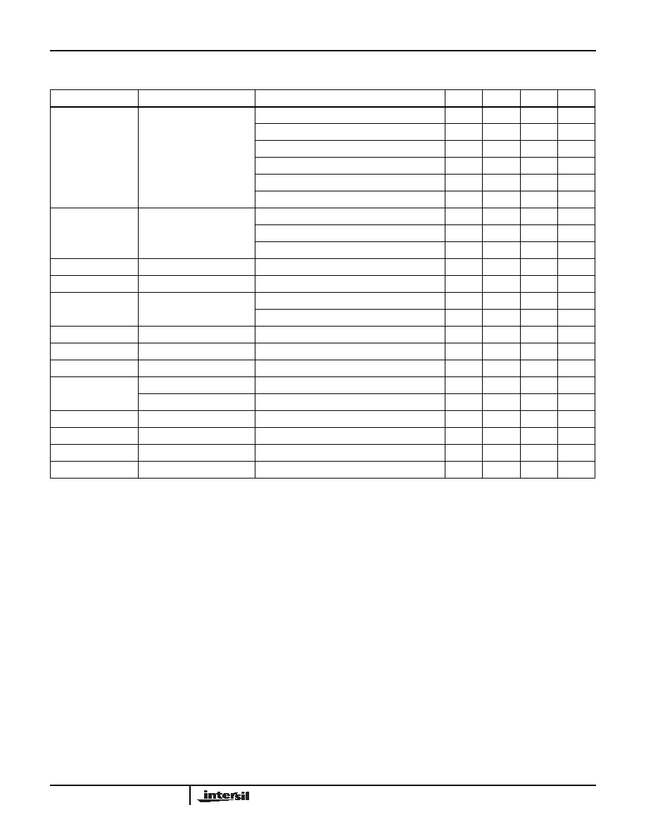
DC Electrical Specifications
V
S
= +5V, GND = 0V, T
A
= 25∞C, V
CM
= +1.5V, V
OUT
= +1.5V, unless otherwise specified.
PARAMETER
DESCRIPTION
TEST CONDITIONS
MIN
TYP
MAX
UNIT
AVOL
Open Loop Gain
V
S
= +12V, V
OUT
= +2V to +9V, R
L
= 1k
to GND
60
80
dB
V
OUT
= +1.5V to +3.5V, R
L
= 1k
to GND
70
dB
V
OUT
= +1.5V to +3.5V, R
L
= 150
to GND
60
dB
V
OP
Positive Output
Voltage Swing
V
S
= +12V, A
V
= +1, R
L
= 1k
to 0V
10.8
V
V
S
= +12V, A
V
= +1, R
L
= 150
to 0V
9.6
10.0
V
V
S
= ±5V, A
V
= +1, R
L
= 1k
to 0V
4.0
V
V
S
= ±5V, A
V
= +1, R
L
= 150
to 0V
3.4
3.8
V
V
S
= +3V, A
V
= +1, R
L
= 150
to 0V
1.8
1.95
V
V
ON
Negative Output
Voltage Swing
V
S
= +12V, A
V
= +1, R
L
= 150
to 0V
5.5
8
mV
V
S
= ±5V, A
V
= +1, R
L
= 1k
to 0V
-4.0
V
V
S
= ±5V, A
V
= +1, R
L
= 150
to 0V
-3.7
-3.4
V
I
OUT
Output Current (Note 1)
V
S
= ±5V, A
V
= +1, R
L
= 10
to 0V
±75
±100
mA
V
S
= ±5V, A
V
= +1, R
L
= 50
to 0V±60VmA
NOTE:
1. Internal short circuit protection circuitry has been built into the EL2250/EL2450; see the Applications section
EL2250, EL2450
4
FN7061.2
June 7, 2005
AC Electrical Specifications
V
S
= +5V, GND = 0V, T
A
= 25∞C, V
CM
= +1.5V, V
OUT
= +1.5V, A
V
= +1, R
F
= 0
, R
L
= 150
to GND pin,
unless otherwise specified. (Note 1)
PARAMETER
DESCRIPTION
TEST CONDITIONS
MIN
TYP
MAX
UNIT
BW
-3dB Bandwidth
(V
OUT
=400mV
P-P
)
V
S
= +5V, A
V
= +1, R
F
= 0
125
MHz
V
S
= +5V, A
V
= -1, R
F
= 500
60
MHz
V
S
= +5V, A
V
= +2, R
F
= 500
60
MHz
V
S
= +5V, A
V
= +10, R
F
= 500
6
MHz
V
S
= +12V, A
V
= +1, R
F
= 0
150
MHz
V
S
= +3V, A
V
= +1, R
F
= 0
100
MHz
BW
±0.1dB Bandwidth
(V
OUT
=400mV
P-P
)
V
S
= +12V, A
V
= +1, R
F
= 0
25
MHz
V
S
= +5V, A
V
= +1, R
F
= 0
30
MHz
V
S
= +3V, A
V
= +1, R
F
= 0
20
MHz
GBWP
Gain Bandwidth Product
V
S
= +12V, @ A
V
= +10
60
MHz
PM
Phase Margin
R
L
= 1k
, C
L
= 6pF
55
∞
SR
Slew Rate
V
S
= +10V, R
L
= 150
, V
OUT
= 0V to +6V
200
275
V/µs
V
S
= +5V, R
L
= 150
, V
OUT
= 0V to +3V
300
V/µs
t
R
, t
F
Rise Time, Fall Time
±0.1V Step
2.8
ns
OS
Overshoot
±0.1V Step
10
%
t
PD
Propagation Delay
±0.1V Step
3.2
ns
t
S
0.1% Settling Time
V
S
= ±5V, R
L
= 500
, A
V
= +1, V
OUT
= ±3V
40
ns
0.01% Settling Time
V
S
= ±5V, R
L
= 500
, A
V
= +1, V
OUT
= ±3V
75
ns
dG
Differential Gain (Note 2)
A
V
= +2, R
F
= 1k
0.05
%
dP
Differential Phase (Note 2)
A
V
= +2, R
F
= 1k
0.05
∞
e
N
Input Noise Voltage
f = 10kHz
48
nV/
Hz
i
N
Input Noise Current
f = 10kHz
1.25
pA/
Hz
NOTES:
1. All AC tests are performed on a "warmed up" part, except slew rate, which is pulse tested
2. Standard NTSC signal = 286mV
P-P
, f = 3.58MHz, as V
IN
is swept from 0.6V to 1.314V; R
L
is DC coupled
EL2250, EL2450

5
FN7061.2
June 7, 2005
Typical Performance Curves
Non-Inverting Frequency
Response (Gain)
Non-Inverting Frequency
Response (Phase)
3dB Bandwidth vs Temperature for
Non-Inverting Gains
3dB Bandwidth vs Temperature for
Inverting Gains
Inverting Frequency Response
(Phase)
Inverting Frequency Response
(Gain)
Frequency Response for Various R
L
Frequency Response for Various C
L
Non-Inverting Frequency
Response vs Common Mode
Voltage
EL2250, EL2450