 | –≠–ª–µ–∫—Ç—Ä–æ–Ω–Ω—ã–π –∫–æ–º–ø–æ–Ω–µ–Ω—Ç: EL2252CM | –°–∫–∞—á–∞—Ç—å:  PDF PDF  ZIP ZIP |

1
Æ
FN7062
CAUTION: These devices are sensitive to electrostatic discharge; follow proper IC Handling Procedures.
1-888-INTERSIL or 321-724-7143
|
Intersil (and design) is a registered trademark of Intersil Americas Inc.
Copyright © Intersil Americas Inc. 2003. All Rights Reserved. Elantec is a registered trademark of Elantec Semiconductor, Inc.
All other trademarks mentioned are the property of their respective owners.
EL2252
Dual 50MHz Comparator/Pin Receiver
The EL2252 dual comparator replaces
the traditional input buffer + attenuator
+ECL comparator +ECL to TTL
translator circuit blocks used in digital equipment. The
EL2252 provides a quick 7ns propagation delay while
complying with ±10V inputs. Input accuracy and propagation
delay is maintained even with input signal Slew Rates as
great as 4000V/µs. The EL2252 can run on supplies as low
as -5.2V and +9V and comply with ECL and CMOS inputs,
or use supplies as great as ±18V for much greater input
range.
The EL2252 has a /TTL pin which, when grounded, restricts
the output V
OH
to a TTL swing to minimize propagation
delay. When left open, the output V
OH
increases to a valid
CMOS level.
The comparators are well behaved and have little tendency
to oscillate over a variety of input and output source and load
impedances. They do not oscillate even when the inputs are
held in the linear range of the device. To improve output
stability in the presence of input noise, an internal 60mV of
hysteresis is available by connecting the HYS pin to V-.
Elantec's products and facilities comply with MIL-I-45208A,
and other applicable quality specifications. For information
on Elantec's processing, see Elantec document, QRA-1;
"Elantec's Processing, Monolithic Integrated Circuits".
Features
∑ Fast response -- 7ns
∑ Inputs tolerate large overdrives with no speed nor bias
current penalties
∑ Propagation delay is relatively constant with variations of
input Slew Rate, overdrive, temperature, and supply
voltage
∑ Output provides proper CMOS or TTL logic levels
∑ Hysteresis is available on-chip
∑ Large voltage gain -- 8000V/V
∑ Not oscillation-prone
∑ Can detect 4ns glitches
∑ MIL-STD-883 Rev. C compliant
Applications
∑ Pin receiver for automatic test equipment
∑ Data communications line receiver
∑ Frequency counter input
∑ Pulse squarer
Ordering Information
PART NUMBER
TEMP. RANGE
PACKAGE
PKG. NO.
EL2252CN
0∞C to +75∞C
14-Pin PDIP
MDP0031
EL2252CM
0∫C to +75∫C
20-Pin SOL
MDP0027
Pinouts
EL2252
(14-PIN PDIP)
TOP VIEW
EL2252
(20-PIN SOL)
TOP VIEW
Data Sheet
December 1995, Rev. E
OBS
OLE
TE P
ROD
UCT
NO R
ECO
MME
NDE
D RE
PLA
CEM
ENT
cont
act o
ur T
echn
ical
Sup
port
Cen
ter a
t
1-88
8-IN
TER
SIL
or w
ww.
inte
rsil.c
om/t
sc
2
Absolute Maximum Ratings
(T
A
= 25∞C)
Voltage between V+ and V- . . . . . . . . . . . . . . . . . . . . . . . . . . . . .36V
Voltage at V+ . . . . . . . . . . . . . . . . . . . . . . . . . . . . . . . . . . . . . . . .18V
Voltage between -IN and +IN pins . . . . . . . . . . . . . . . . . . . . . . . .36V
Output Current . . . . . . . . . . . . . . . . . . . . . . . . . . . . . . . . . . . . . 12mA
Current into +IN,-IN, HYS or /TTL . . . . . . . . . . . . . . . . . . . . . . . 5mA
Internal Power Dissipation . . . . . . . . . . . . . . . . . . . . . . . See Curves
Operating Ambient Temperature Range . . . . . . . . . . -25∞C to +85∞C
Operating Junction Temperature . . . . . . . . . . . . . . . . . . . . . . . 150∞C
Storage Temperature Range . . . . . . . . . . . . . . . . . . . . -65∞ to +150C
CAUTION: Stresses above those listed in "Absolute Maximum Ratings" may cause permanent damage to the device. This is a stress only rating and operation of the
device at these or any other conditions above those indicated in the operational sections of this specification is not implied.
IMPORTANT NOTE: All parameters having Min/Max specifications are guaranteed. Typical values are for information purposes only. Unless otherwise noted, all tests
are at the specified temperature and are pulsed tests, therefore: T
J
= T
C
= T
A
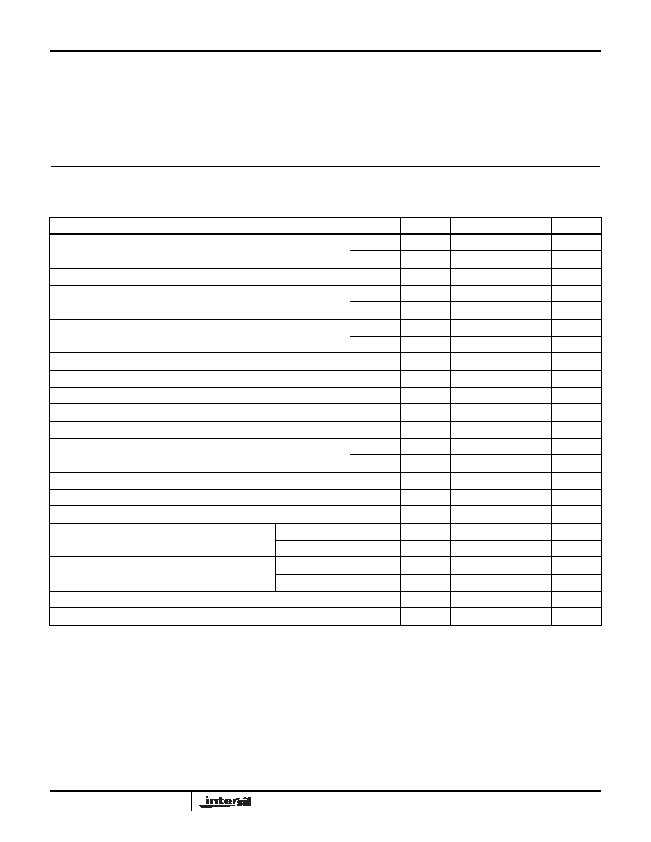
DC Electrical Specifications
V
S
= ±15V; HYS and /TTL grounded; T
A
= 25∞C unless otherwise specified.
PARAMETER
DESCRIPTION
TEMP
MIN
TYP
MAX
UNITS
V
OS
Input Offset Voltage
25∞C
1
9
mV
Full
13
mV
TCV
OS
Average Offset Voltage Drift
Full
7
µV/C
I
B
Input Bias Current at Null
25∞C
6
16
µA
Full
21
µA
I
OS
Input Offset Current
25∞C
0.2
1
µA
Full
2
µA
R
IN
, diff
Input Differential Resistance
25∞C
30
k
R
IN
, comm
Input Common-Mode Resistance
25∞C
10
M
C
IN
Input Capacitance
25∞C
2
pF
V
CM
+
Positive Common-Mode Input Range
Full
10
13
V
V
CM
-
Negative Common-Mode Input Range
Full
-9
-12
V
A
VOL
Large Signal Voltage Gain
VO = 0.8V to 2.0V
25∞C
4000
8000
V/V
Full
3000
V/V
CMRR
Common-Mode Rejection Ratio (Note 1)
Full
70
95
II
PSRR
Power-Supply Rejection Ratio (Note 2)
Full
70
90
II
V
HYS
Peak-to-Peak Input Hysteresis with HYS connected to V-
25∞C
60
V
V
OH
High Level Output
CMOS Mode
Full
4.0
4.6
5.1
V
TTL Mode
Full
2.4
2.7
3.2
V
V
OL
Low Level Output
I1 = 0
Full
-0.2
0.2
0.8
V
I1 = 5mA
Full
-0.2
0.4
0.8
V
I
S
+
Positive Supply Current
Full
16
19
II
I
S
-
Negative Supply Current
Full
17
20
II
NOTES:
1. Two tests are performed with V
CM
= 0V to -9V and V
CM
= 0V to 10V.
2. Two tests are performed with V+ = 15V, V- changed from -10V to -15V; V- = -15V, V+ changed from 10V to 15V.
EL2252

3
AC Test Circuit
Burn-In Circuit
AC Electrical Specifications
V
S
= ±15V; C
L
= 10pF; T
A
= 25∞C; TTL output threshold is 1.4V, CMOS output threshold is 2.5V; unless
otherwise specified.
PARAMETER
DESCRIPTION
MIN
TYP
MAX
UNITS
T
PD+
, T
PD-
Input to Output Propagation Delay,
0 < V
IN
< 5V, 500mV Overdrive,
2000V/µs Input Slew Rate
TTL Output Swing
6
9
ns
CMOS Output Swing
8
ns
T
PD+
, T
PD-
Input to Output Propagation Delay,
-2V < V
IN
< -1V, 500mV Overdrive,
2ns Input Rise Time
TTL Output Swing
5
9
ns
CMOS Output Swing
9
ns
T
PDSYM
Propagation Delay Change between Positive and Negative
Input Slopes
1.25
ns
EL2252

4
Typical Performance Curves
Input/Output Transfer Function - HYS Open
Input/Output Transfer Function - HYS Connected to V
Input Bias Current
vs Small Overdrives
Input Bias Current
vs Large Overdrives
Input Hysteresis Voltage
vs Temperature
Bias Current vs
Temperature Inputs Balanced
/TTL
open
/TTL
grounded
-Gnd
# OV-
(/TTL
open)
-Gnd
EL2252

5
Typical Performance Curves
(Continued)
Supply Current vs Supply Voltage
Supply Current vs Temperature
(Vs = ±15V)
Output Delay -- 0.5V Overdrive
Output Delay -- 0.5V Overdrive
Output with 50MHz CMOS Input
Output with 50MHz ECL Input
CMOS out
TTL out
1v/div
Input Gnd
CMOS
out
TTL
out
1v/div
Gnd
Gnd
1v/div
Gnd
1v/div
4ns TTL Glitch Detection
1v/div
Gnd
EL2252