1
Æ
FN7063
CAUTION: These devices are sensitive to electrostatic discharge; follow proper IC Handling Procedures.
1-888-INTERSIL or 321-724-7143
|
Intersil (and design) is a registered trademark of Intersil Americas Inc.
Copyright © Intersil Americas Inc. 2003. All Rights Reserved. Elantec is a registered trademark of Elantec Semiconductor, Inc.
All other trademarks mentioned are the property of their respective owners.
EL2257
125MHz Single Supply, Clamping Op Amp
The EL2257 is a single supply op amp.
Prior single supply op amps have
generally been limited to bandwidths
and slew rates one-fourth of that of the EL2257. The
125MHz bandwidth, 275V/µs slew rate and 0.05%/0.05∞
differential gain/differential phase makes this part ideal for
single or dual supply video speed applications. With its
voltage feedback architecture, this amplifier can accept
reactive feedback networks, allowing them to be used in
analog filtering applications. The inputs can sense signals
below the bottom supply rail and as high as 1.2V below the
top rail. Connecting the load resistor to ground and operating
from a single supply, the outputs swing completely to ground
without saturating. The outputs can also drive to within 1.2V
of the top rail. The EL2257 will output ±100mA and will
operate with single supply voltages as low as 2.7V, making
them ideal for portable, low power applications.
The EL2257 has a high speed disable feature. Applying a
low logic level to all ENABLE pins reduces the supply current
to 0µA within 50ns. Each amplifier has its own ENABLE pin.
This is useful for both multiplexing and reducing power
consumption.
The EL2257 also has an output voltage clamp feature. This
clamp is a fast recovery (< 7ns) output clamp that prevents
the output voltage from going above the preset clamp
voltage. This feature is desirable for A/D applications, as A/D
converters can require long times to recover if overdriven.
The EL2257 is available in 14-pin SO (0.150") and 14-pin
PDIP packages and operates over the industrial temperature
range of -40∞C to +85∞C. For single amplifier applications,
see the EL2150 and EL2157. For space-saving, industry-
standard pinout dual and quad applications, see the EL2250
and EL2450.
Features
∑ Specified for +3V, +5V, or ± 5V applications
∑ Power-down to 0µA
∑ Output voltage clamp
∑ Large input common-mode range 0V < V
CM
< V
S
- 1.2V
∑ Output swings to ground without saturating
∑ -3dB bandwidth = 125MHz
∑ ±0.1dB bandwidth = 30MHz
∑ Low supply current = 5mA
∑ Slew rate = 275V/µs
∑ Low offset voltage = 4mV max
∑ Output current = ±100mA
∑ High open loop gain = 80dB
∑ Differential gain = 0.05%
∑ Differential phase = 0.05∞
Applications
∑ Video amplifiers
∑ PCMCIA applications
∑ A/D drivers
∑ Line drivers
∑ Portable computers
∑ High speed communications
∑ RGB printer, fax, scanner applications
∑ Broadcast equipment
∑ Active filtering
∑ Multiplexing
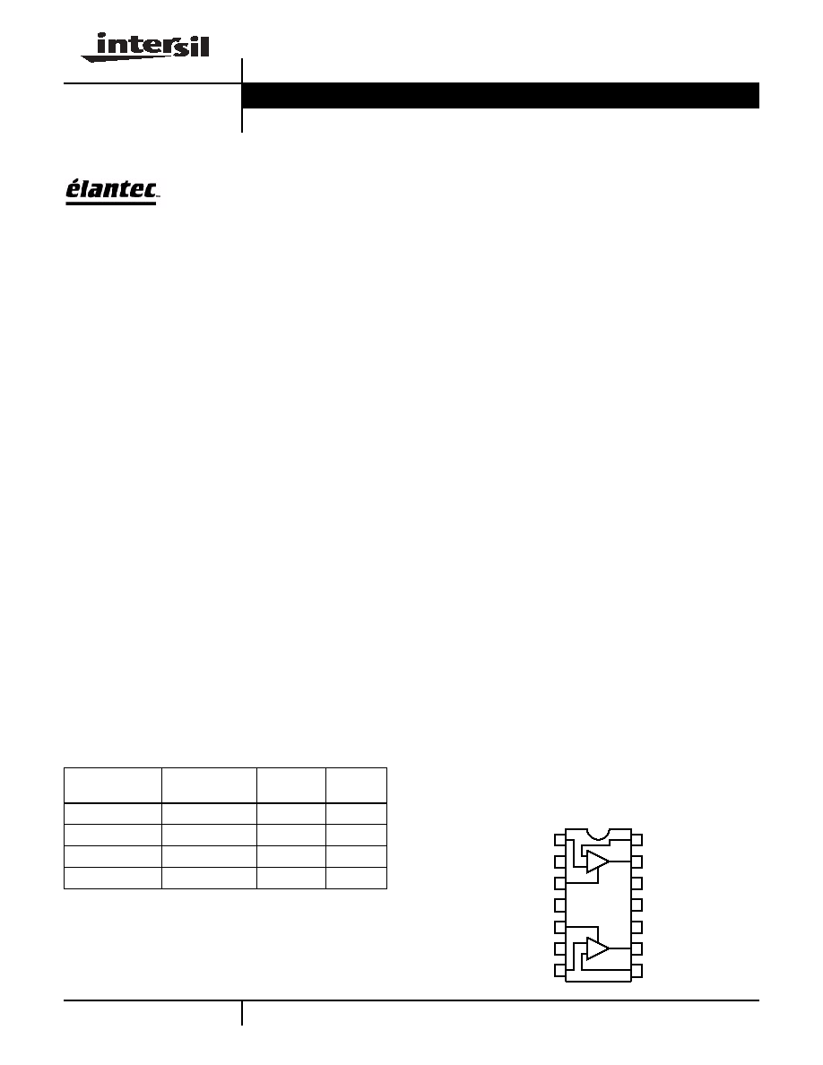
Pinout
EL2257
[14-PIN SO (0.150"), PDIP]
TOP VIEW
Ordering Information
PART NUMBER
PACKAGE
TAPE &
REEL
PKG. NO.
EL2257CS
14-Pin SO (0.150")
-
MDP0027
EL2257CS-T7
14-Pin SO (0.150")
7"
MDP0027
EL2257CS-T13
14-Pin SO (0.150")
13"
MDP0027
EL2257CN
14-Pin PDIP
-
MDP0031
1
2
3
4
14
13
12
11
5
6
7
10
9
8
-
+
-
+
INA+
CLAMPA
ENABLEA
GND
ENABLEB
CLAMPB
INB+
INA-
OUTA
NC
VS+
NC
OUTB
INB-
Data Sheet
February 28, 2002
2
Absolute Maximum Ratings
(T
A
= 25∞C)
Supply Voltage between V
S
and GND . . . . . . . . . . . . . . . . . . . 12.6V
Input Voltage (I
N
+, I
N
-, ENABLE, CLAMP) . . . GND≠0.3V, V
S
+0.3V
Differential Input Voltage . . . . . . . . . . . . . . . . . . . . . . . . . . . . . . .±6V
Maximum Output Current. . . . . . . . . . . . . . . . . . . . . . . . . . . . . 90mA
Output Short Circuit Duration. . . . . . . . . . . . . . . . See Note 1 page 3
Power Dissipation . . . . . . . . . . . . . . . . . . . . . . . . . . . . . . See curves
Storage Temperature Range . . . . . . . . . . . . . . . . . . -65∞C to +150∞C
Ambient Operating Temperature Range . . . . . . . . . . -40∞C to +85∞C
Operating Junction Temperature . . . . . . . . . . . . . . . . . . . . . . +150∞C
CAUTION: Stresses above those listed in "Absolute Maximum Ratings" may cause permanent damage to the device. This is a stress only rating and operation of the
device at these or any other conditions above those indicated in the operational sections of this specification is not implied.
IMPORTANT NOTE: All parameters having Min/Max specifications are guaranteed. Typical values are for information purposes only. Unless otherwise noted, all tests
are at the specified temperature and are pulsed tests, therefore: T
J
= T
C
= T
A
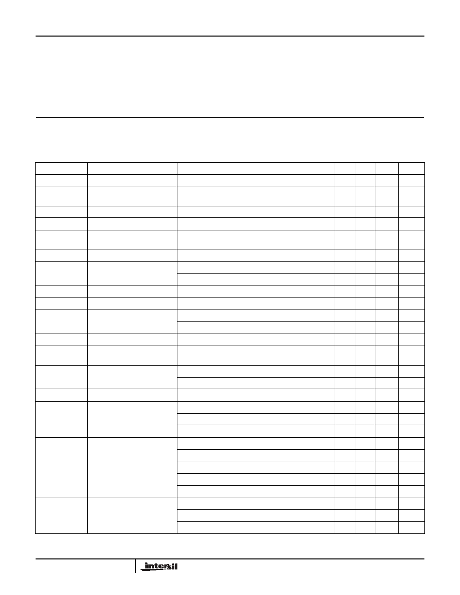
DC Electrical Specifications
V
S
= +5V, GND = 0V, T
A
= 25∞C, V
CM
= 1.5V, V
OUT
= 1.5V, V
CLAMP
= +5V, V
ENABLE
= +5V, unless
otherwise specified.
PARAMETER
DESCRIPTION
CONDITIONS
MIN
TYP
MAX
UNIT
V
OS
Offset Voltage
-4
4
mV
TCV
OS
Offset Voltage Temperature
Coefficient
Measured from T
MIN
to T
MAX
10
µV/∞C
IB
Input Bias Current
V
IN
= 0V
-5.5
-10
µA
I
OS
Input Offset Current
V
IN
= 0V
-1100
150
+1100
nA
TCI
OS
Input Bias Current Temperature
Coefficient
Measured from T
MIN
to T
MAX
50
nA/∞C
PSRR
Power Supply Rejection Ratio
V
S
= V
ENABLE
= 2.7V to 12V, V
CLAMP
= OPEN
45
70
dB
CMRR
Common-mode Rejection Ratio
V
CM
= 0V to +3.8V
50
65
dB
V
CM
= 0V to +3.0V
55
70
dB
CMIR
Common-mode Input Range
0
V
S
-1.2
V
R
IN
Input Resistance
Common-mode
1
2
M
C
IN
Input Capacitance
SO (0.150") package
1
pF
PDIP package
1.5
pF
R
OUT
Output Resistance
A
V
= +1
40
m
I
SON
Supply Current - Enabled (per
amplifier)
V
S
= V
CLAMP
= 12V, V
ENABLE
= 12V
5
6.5
mA
I
SOFF
Supply Current - Shut-down (per
amplifier)
V
S
= V
CLAMP
= 10V, V
ENABLE
= 0.5V
0
50
µA
V
S
= V
CLAMP
= 12V, V
ENABLE
= 0.5V
5
µA
PSOR
Power Supply Operating Range
2.7
12.0
V
AVOL
Open Loop Gain
V
S
= V
CLAMP
= 12V, V
OUT
= 2V to 9V, R
L
= 1k
to GND
65
80
dB
V
OUT
= 1.5V to 3.5V, R
L
= 1k
to GND
70
dB
V
OUT
= 1.5V to 3.5V, R
L
= 150
to GND
60
dB
V
OP
Positive Output Voltage Swing
V
S
= 12V, A
V
= 1, R
L
= 1k
to 0V
10.8
V
V
S
= 12V, A
V
= 1, R
L
= 150
to 0V
9.6
10.0
V
V
S
= ±5V, A
V
= 1, R
L
= 1k
to 0V
4.0
V
V
S
= ±5V, A
V
= 1, R
L
= 150
to 0V
3.4
3.8
V
V
S
= 3V, A
V
= 1, R
L
= 150
to 0V
1.8
1.95
V
V
ON
Negative Output Voltage Swing
V
S
= 12V, A
V
= 1, R
L
= 150
to 0V
5.5
8
mV
V
S
= ±5V, A
V
= 1, R
L
= 1k
to 0V
-4.0
V
V
S
= ±5V, A
V
= 1, R
L
= 150
to 0V
-3.7
-3.4
V
EL2257

3
I
OUT
Output Current (Note 1)
V
S
= ±5V, A
V
= 1, R
L
= 10
to 0V
±75
±100
mA
V
S
= ±5V, A
V
= 1, R
L
= 50
to 0V
±60
mA
I
OUT,OFF
Output Current - Disabled
V
ENABLE
= 0.5V
0
20
µA
V
IH-EN
ENABLE Pin Voltage for Power-
up
Relative to GND pin
2.0
V
V
IL-EN
ENABLE Pin Voltage for Shut-
down
Relative to GND pin
0.5
V
I
IH-EN
ENABLE Pin Input Current -
High(Note 2)
V
S
= V
CLAMP
= 12V, V
ENABLE
= 12V
340
410
µA
I
IL-EN
ENABLE Pin Input Current - Low
(Note 2)
V
S
= V
CLAMP
= 12V, V
ENABLE
= 0.5V
0
1
µA
V
OR-CL
Voltage Clamp Operating
Range (Note 3)
Relative to GND pin
1.2
V
OP
V
V
ACC-CL
CLAMP Accuracy (Note 4)
V
IN
= 4V, R
L
= 1k
to GND, V
CLAMP
= 1.5V and 3.5V
-250
100
250
mV
I
IH-CL
CLAMP Pin Input Current - High V
S
= V
CLAMP
= 12V
12
25
µA
I
IL-CL
CLAMP Pin Input Current - Low
(per amp)
V
S
= 12V, V
CLAMP
= 1.2V
-30
-15
µA
NOTES:
1. Internal short circuit protection circuitry has been built into the EL2257. See the Applications section.
2. If the disable feature is not desired, tie the ENABLE pins to the V
S
pin, or apply a logic high level to the ENABLE pins.
3. The maximum output voltage that can be clamped is limited to the maximum positive output Voltage, or V
OP
. Applying a voltage higher than V
OP
inactivates the clamp. If the clamp feature is not desired, either tie the CLAMP pin to the V
S
pin, or simply let the CLAMP pin float.
4. The clamp accuracy is affected by V
IN
and R
L
. See the Typical Curves Section and the Clamp Accuracy vs V
IN
and R
L
curve.
DC Electrical Specifications
V
S
= +5V, GND = 0V, T
A
= 25∞C, V
CM
= 1.5V, V
OUT
= 1.5V, V
CLAMP
= +5V, V
ENABLE
= +5V, unless
otherwise specified. (Continued)
PARAMETER
DESCRIPTION
CONDITIONS
MIN
TYP
MAX
UNIT
Closed Loop AC Electrical Specifications
V
S
= +5V, GND = 0V, T
A
= 25∞C, V
CM
= +1.5V, V
OUT
= +1.5V, V
CLAMP
= +5V, V
ENABLE
= +5V, A
V
= +1, R
F
= 0
, R
L
= 150
to GND pin unless otherwise specified. (Note 1)
PARAMETER
DESCRIPTION
CONDITIONS
MIN TYP
MAX
UNIT
BW
-3dB Bandwidth
(V
OUT
= 400mV
P-P
)
V
S
= 5V, A
V
= 1, R
F
= 0
125
MHz
V
S
= 5V, A
V
= -1, R
F
= 500
60
MHz
V
S
= 5V, A
V
= 2, R
F
= 500
60
MHz
V
S
= 5V, A
V
= 10, R
F
= 500
6
MHz
V
S
= 12V, A
V
= 1, R
F
= 0
150
MHz
V
S
= 3V, A
V
= 1, R
F
= 0
100
MHz
BW
±0.1dB Bandwidth
(V
OUT
= 400mV
P-P
)
V
S
= 12V, A
V
= 1, R
F
= 0
25
MHz
V
S
= 5V, A
V
= 1, R
F
= 0
30
MHz
V
S
= 3V, A
V
= 1, R
F
= 0
20
MHz
GBWP
Gain Bandwidth Product
V
S
= 12V, @ A
V
= 10
60
MHz
PM
Phase Margin
R
L
= 1k
, C
L
= 6pF
55
∞
SR
Slew Rate
V
S
= 10V, R
L
= 150
, V
OUT
= 0V to 6V
200
275
V/µs
V
S
= 5V, R
L
= 150
, V
OUT
= 0V to +3V
300
V/µs
t
R
,t
F
Rise Time, Fall Time
±0.1V step
2.8
ns
OS
Overshoot
±0.1V step
10
%
t
PD
Propagation Delay
±0.1V step
3.2
ns
EL2257
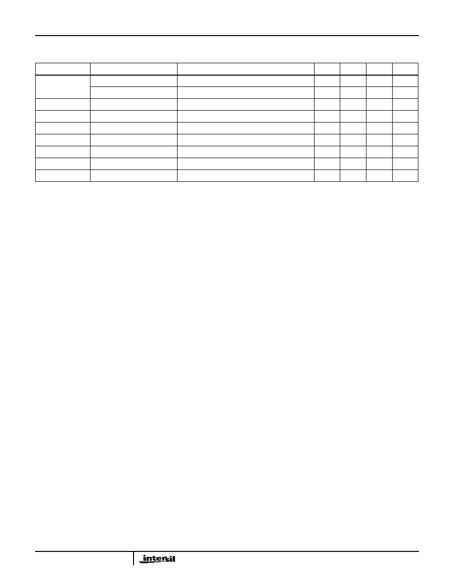
4
t
S
0.1% Settling Time
V
S
= ±5V, R
L
= 500
, A
V
= 1, V
OUT
= ±3V
40
ns
0.01% Settling Time
V
S
= ±5V, R
L
= 500
, A
V
= 1, V
OUT
= ±3V
75
ns
dG
Differential Gain (Note 2)
A
V
= 2, R
F
= 1k
0.05
%
dP
Differential Phase (Note 2)
A
V
= 2, R
F
= 1k
0.05
∞
e
N
Input Noise Voltage
f = 10kHz
48
nV/
Hz
i
N
Input Noise Current
f = 10kHz
1.25
pA/
Hz
t
DIS
Disable Time (Note 3)
50
ns
t
EN
Enable Time (Note 3)
25
ns
t
CL
Clamp Overload Recovery
7
ns
NOTES:
1. All AC tests are performed on a "warmed up" part, except slew rate, which is pulse tested.
2. Standard NTSC signal = 286mV
P-P
, f = 3.58MHz, as V
IN
is swept from 0.6V to 1.314V. R
L
is DC coupled.
3. Disable/Enable time is defined as the time from when the logic signal is applied to the ENABLE pin to when the supply current has reached half
its final value.
Closed Loop AC Electrical Specifications
V
S
= +5V, GND = 0V, T
A
= 25∞C, V
CM
= +1.5V, V
OUT
= +1.5V, V
CLAMP
= +5V, V
ENABLE
= +5V, A
V
= +1, R
F
= 0
, R
L
= 150
to GND pin unless otherwise specified. (Note 1)
PARAMETER
DESCRIPTION
CONDITIONS
MIN TYP
MAX
UNIT
EL2257

5
Typical Performance Curves
Non-Inverting Frequency
Response (Gain)
Non-Inverting Frequency
Response (Phase)
3dB Bandwidth vs Temperature for
Non-Inverting Gains
3dB Bandwidth vs Temperature for
Inverting Gains
Inverting Frequency Response (Phase)
Inverting Frequency Response (Gain)
Frequency Response for Various R
L
Frequency Response for Various C
L
Non-Inverting Frequency Response vs
Common Mode Voltage
EL2257