1
Æ
FN7054.1
EL2276
70MHz/1mA Current Mode Feedback Amp
w/Disable
The EL2276 is a dual current-feedback operational amplifier
which achieves a -3dB bandwidth of 70MHz at a gain of +1
while consuming only 1mA of supply current per amplifier. It
will operate with dual supplies ranging from ±1.5V to ±6V, or
from single supplies ranging from +3V to +12V. The EL2276
also includes a disable/power-down feature which reduces
current consumption to 0mA while placing the amplifier
output in a high impedance state. In spite of its low supply
current, the EL2276 can output 55mA while swinging to ±4V
on ±5V supplies. These attributes make the EL2276
excellent choice for low power and/or low voltage cable-
driver, HDSL, or RGB applications.
Features
∑ Dual topology
∑ 1mA supply current (per amplifier)
∑ 70MHz -3dB bandwidth
∑ Low cost
∑ Fast disable
∑ Powers down to 0mA
∑ Single- and dual-supply operation down to ±1.5V
∑ 0.15%/0.15∞ diff. gain/diff. phase into 150
∑ 800V/µs slew rate
∑ Large output drive current: 55mA
∑
Pb-Free available (RoHS compliant)
Applications
∑ Low power/battery applications
∑ HDSL amplifiers
∑ Video amplifiers
∑ Cable drivers
∑ RGB amplifiers
∑ Test equipment amplifiers
∑ Current to voltage converters
Ordering Information
PART NUMBER
PACKAGE
TAPE & REEL PKG. DWG. #
EL2276CS
14-Pin SOIC
-
MDP0027
EL2276CS-T7
14-Pin SOIC
7"
MDP0027
EL2276CS-T13
14-Pin SOIC
13"
MDP0027
EL2276CSZ
(See Note)
14-Pin SOIC
(Pb-free)
-
MDP0027
EL2276CSZ-T7
(See Note)
14-Pin SOIC
(Pb-free)
7"
MDP0027
EL2276CSZ-T13
(See Note)
14-Pin SOIC
(Pb-free)
13"
MDP0027
NOTE: Intersil Pb-free products employ special Pb-free material sets;
molding compounds/die attach materials and 100% matte tin plate
termination finish, which are RoHS compliant and compatible with
both SnPb and Pb-free soldering operations. Intersil Pb-free products
are MSL classified at Pb-free peak reflow temperatures that meet or
exceed the Pb-free requirements of IPC/JEDEC J STD-020.
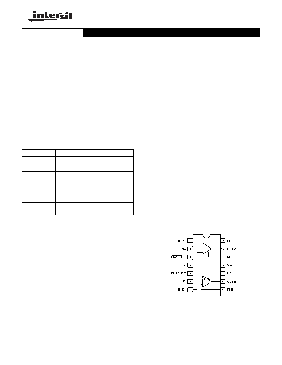
Pinout
EL2276
(14-PIN SO)
TOP VIEW
Manufactured under U.S. Patent No. 5,352,989, 5,351,012,
5,418,495
Data Sheet
May 6, 2005
CAUTION: These devices are sensitive to electrostatic discharge; follow proper IC Handling Procedures.
1-888-INTERSIL or 1-888-352-6832
|
Intersil (and design) is a registered trademark of Intersil Americas Inc.
Copyright Intersil Americas Inc. 1995, 2003, 2005. All Rights Reserved
All other trademarks mentioned are the property of their respective owners.
2
Absolute Maximum Ratings
(T
A
= 25∞C)
Voltage between V
S
+ and V
S
-. . . . . . . . . . . . . . . . . . . . . . . . +12.6V
Common-Mode Input Voltage . . . . . . . . . . . . . . . . . . . . . V
S
- to V
S
+
Differential Input Voltage . . . . . . . . . . . . . . . . . . . . . . . . . . . . . . .±6V
Current into +IN or -IN . . . . . . . . . . . . . . . . . . . . . . . . . . . . . .±7.5mA
Internal Power Dissipation . . . . . . . . . . . . . . . . . . . . . . . See Curves
Operating Ambient Temperature Range . . . . . . . . . .-40∞C to +85∞C
Operating Junction Temperature Plastic Packages. . . . . . . . . 150∞C
Output Current (EL2276) . . . . . . . . . . . . . . . . . . . . . . . . . . . . ±60mA
Storage Temperature Range . . . . . . . . . . . . . . . . . .-65∞C to +150∞C
CAUTION: Stresses above those listed in "Absolute Maximum Ratings" may cause permanent damage to the device. This is a stress only rating and operation of the
device at these or any other conditions above those indicated in the operational sections of this specification is not implied.
IMPORTANT NOTE: All parameters having Min/Max specifications are guaranteed. Typical values are for information purposes only. Unless otherwise noted, all tests
are at the specified temperature and are pulsed tests, therefore: T
J
= T
C
= T
A
DC Electrical Specifications
V
S
= ±5V, R
L
= 150
, ENABLE = 0V, T
A
= 25∞C unless otherwise specified.
PARAMETER
DESCRIPTION
CONDITIONS
MIN
TYP
MAX
UNITS
V
OS
Input Offset Voltage
2.5
15
mV
TCV
OS
Average Input Offset Voltage Drift
Measured from T
MIN
to T
MAX
5
µV/∞C
dV
OS
V
OS
Matching
0.5
mV
+I
IN
+ Input Current
0.5
5
µA
d+I
IN
+I
IN
Matching
20
nA
-I
IN
- Input Current
4
15
µA
d-I
IN
-I
IN
Matching
1.5
µA
CMRR
Common Mode Rejection Ratio
V
CM
= ±3.5 V
45
50
dB
-ICMR
- Input Current Common Mode Rejection
V
CM
= ±3.5V
4
10
µA/V
PSRR
Power Supply Rejection Ratio
V
S
is moved from ±4V to ±6V
60
70
dB
-IPSR
- Input Current Power Supply Rejection
V
S
is moved from ±4V to ±6V
0.5
5
µA/V
R
OL
Transimpedance
V
OUT
= ±2.5V
150
400
k
+R
IN
+ Input Resistance
V
CM
= ±3.5V
1
4
M
+C
IN
+ Input Capacitance
1.2
pF
CMIR
Common Mode Input Range
±3.5
±4.0
V
V
O
Output Voltage Swing
V
S
= ±5
±3.5
±4.0
V
V
S
= +5 Single-Supply, High
4.0
V
V
S
= +5 Single-Supply, Low
0.3
V
I
O
Output Current
Per Amplifier
50
55
mA
I
S
Supply Current
ENABLE = 2.0V, per Amplifier
1
2
mA
I
S(DIS)
Supply Current (Disabled)
ENABLE = 4.5V
0
20
µA
C
OUT(DIS)
Output Capacitance (Disabled)
ENABLE = 4.5V
4.4
pF
R
EN
Enable Pin Input Resistance
Measured at ENABLE = 2.0V, 4.5V
45
85
k
I
IH
Logic "1" Input Current
Measured at ENABLE, ENABLE = 4.5V
-0.04
µA
I
IL
Logic "0" Input Current
Measured at ENABLE, ENABLE = 0V
-53
µA
V
DIS
Minimum Voltage at ENABLE to Disable
4.5
V
V
EN
Maximum Voltage at ENABLE to Enable
2.0
V
EL2276
3
AC Electrical Specifications
V
S
= ±5V, R
F
= R
G
= 1.0k
, R
L
= 150
, ENABLE = 0V, T
A
= 25∞C unless otherwise specified.
PARAMETER
DESCRIPTION
CONDITIONS
MIN
TYP
MAX
UNITS
-3dB BW
-3dB Bandwidth
A
V
= +1
70
MHz
-3dB BW
-3dB Bandwidth
A
V
= +2
60
MHz
SR
Slew Rate
V
OUT
= ±2.5V, A
V
= +2
400
800
V/µs
t
R
, t
F
Rise and Fall Time
V
OUT
= ±500mV
4.5
ns
t
PD
Propagation Delay
V
OUT
= ±50mV
4.5
ns
OS
Overshoot
V
OUT
= ±500mV
3.0
%
ts
0.1% Settling
V
OUT
= ±2.5V, A
V
= -1
40
ns
dG
Differential Gain
A
V
= +2, R
L
= 150
(Note 1)
0.15
%
dP
Differential Phase
A
V
= +2, R
L
= 150
(Note 1)
0.15
∞
dG
Differential Gain
A
V
= +1, R
L
= 500
(Note 1)
0.02
%
dP
Differential Phase
A
V
= +1, R
L
= 500
(Note 1)
0.01
∞
t
ON
Turn-On Time
A
V
= +2, V
IN
= +1V, R
L
= 150
(Note 2)
40
100
ns
t
OFF
Turn-Off Time
A
V
= +2, V
IN
= +1V, R
L
= 150
(Note 2)
1500
2000
ns
CS
Channel Separation
f = 5MHz
85
dB
NOTES:
1. DC offset from 0V to 0.714V, AC amplitude 286mV
P-P
, f = 3.58MHz.
2. Measured from the application of the logic signal until the output voltage is at the 50% point between initial and final values.
EL2276
4
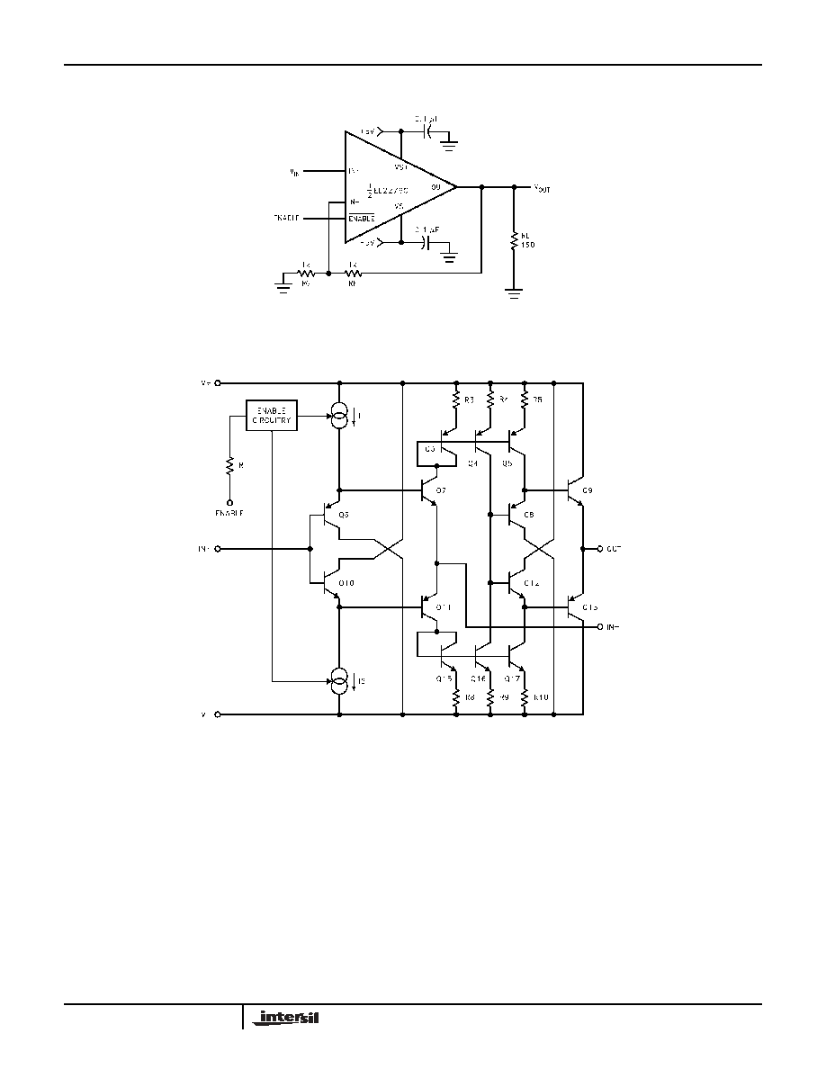
Test Circuit
(per Amplifier)
Simplified Schematic
(per Amplifier)
EL2276
5
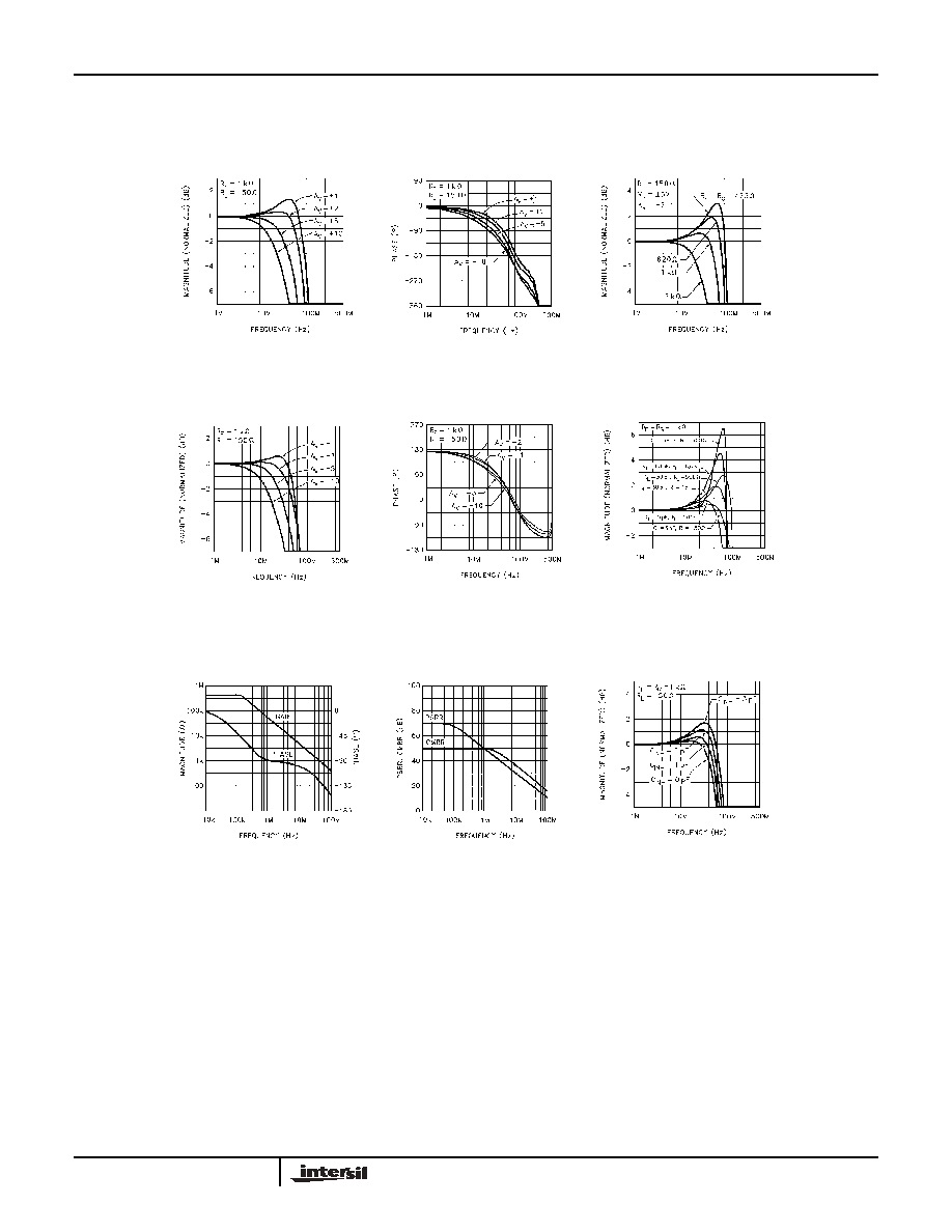
Typical Performance Curves
Non-Inverting
Frequency Response (Gain)
Non-Inverting
Frequency Response (Phase)
Frequency Response for
Various R
F
and R
G
Inverting Frequency
Response (Gain)
Transimpedance (R
OL
)
PSRR and CMRR
Frequency Response
for Various C
IN
-
Frequency Response for
Various R
L
and C
L
Inverting Frequency
Response (Phase)
EL2276