 | –≠–ª–µ–∫—Ç—Ä–æ–Ω–Ω—ã–π –∫–æ–º–ø–æ–Ω–µ–Ω—Ç: EL2344 | –°–∫–∞—á–∞—Ç—å:  PDF PDF  ZIP ZIP |
1
Æ
FN7154
CAUTION: These devices are sensitive to electrostatic discharge; follow proper IC Handling Procedures.
1-888-INTERSIL or 321-724-7143
|
Intersil (and design) is a registered trademark of Intersil Americas Inc.
Copyright © Intersil Americas Inc. 2003. All Rights Reserved. Elantec is a registered trademark of Elantec Semiconductor, Inc.
All other trademarks mentioned are the property of their respective owners.
EL2344
Triple Low-Power 60MHz Unity-Gain
Stable Op Amp
The EL2344 is a triple version of the
popular EL2044. It is a high speed, low
power, low cost monolithic operational
amplifier built on Elantec's proprietary complementary
bipolar process. The EL2344 is unity-gain stable and feature
a 325V/µs slew rate and 60MHz gain-bandwidth product
while requiring only 5.2mA of supply current per amplifier.
The power supply operating range of the EL2344 is from
±18V down to as little as ±2V. For single-supply operation,
the EL2344 operates from 36V down to as little as 2.5V. The
excellent power supply operating range of the EL2344
makes it an obvious choice for applications on a single +5V
or +3V supply.
The EL2344 also features an extremely wide output voltage
swing of ±13.6V with V
S
= ±15V and R
L
= 1000
. At ±5V,
output voltage swing is a wide ±3.8V with R
L
= 500
and
±3.2V with R
L
= 150
. Furthermore, for single-supply
operation at +5V, output voltage swing is an excellent 0.3V to
3.8V with R
L
= 500
.
At a gain of +1, the EL2344 has a -3dB bandwidth of
120MHz with a phase margin of 50∞. It can drive unlimited
load capacitance, and because of its conventional voltage-
feedback topology, the EL2344 allows the use of reactive or
non-linear elements in their feedback network. This
versatility combined with low cost and 75mA of output-
current drive makes the EL2344 an ideal choice for price-
sensitive applications requiring low power and high speed.
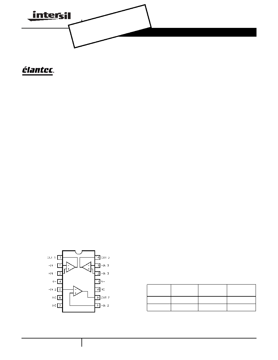
Pinout
Features
∑ 60MHz gain-bandwidth product
∑ Unity-gain stable
∑ Low supply current (per Amplifier)
- 5.2mA at V
S
= ±15V
∑ Wide supply range
- ±2V to ±18V dual-supply
- 2.5V to 36V single-supply
∑ High slew rate = 325V/µs
∑ Fast settling = 80ns to 0.1% for a 10V step
∑ Low differential gain = 0.04% at A
V
= +2, R
L
= 150
∑ Low differential phase = 0.15∞ at A
V
= +2, R
L
= 150
∑ Stable with unlimited capacitive load
∑ Wide output voltage swing
- 13.6V with V
S
= ±15V, R
L
= 1000
- 3.8V/0.3V with V
S
= +5V, R
L
= 500
∑ Low cost, enhanced replacement for the AD827 and
LT1229/LT1230
Applications
∑ Video amplifier
∑ Single-supply amplifier
∑ Active filters/integrators
∑ High-speed sample-and-hold
∑ High-speed signal processing
∑ ADC/DAC buffer
∑ Pulse/RF amplifier
∑ Pin diode receiver
∑ Log amplifier
∑ Photo multiplier amplifier
∑ Difference amplifier
EL2344
14-PIN PDIP, SO
TOP VIEW
Ordering Information
PART
NUMBER
TEMP. RANGE
PACKAGE
PKG. NO.
EL2344CN
-40∞C to +85∞C
14-Pin PDIP
MDP0031
EL2344CS
-40∞C to +85∞C
14-Pin SO
MDP0027
Data Sheet
September 1996, Rev. A
OBS
OLET
E PR
ODU
CT
NO R
ECO
MME
NDED
REP
LACE
MEN
T
conta
ct ou
r Tec
hnica
l Sup
port
Cent
er at
1-888
-INTE
RSIL
or ww
w.int
ersil.
com/
tsc

2
Absolute Maximum Ratings
(T
A
= 25 ∞C)
Supply Voltage (V
S
) . . . . . . . . . . . . . . . . . . . . . . . . . . . . ±18V or 36V
Peak Output Current (I
OP
) . . . . . . . . . . . . . . .Short-Circuit Protected
Output Short-Circuit Duration (Note 1) . . . . . . . . . . . . . . . . . Infinite
Input Voltage (V
IN
) . . . . . . . . . . . . . . . . . . . . . . . . . . . . . . . . . . . ±V
S
Differential Input Voltage (V
IN
) . . . . . . . . . . . . . . . . . . . . . . . . . .±10V
Power Dissipation (P
D
) . . . . . . . . . . . . . . . . . . . . . . . . . See Curves
Operating Temperature Range (T
A
) . . . . . . . . . . . . . . -40∞C to +85∞C
Operating Junction Temperature (T
J
) . . . . . . . . . . . . . . . . . . . 150∞C
Storage Temperature (T
ST
) . . . . . . . . . . . . . . . . . . . -65∞C to +150∞C
CAUTION: Stresses above those listed in "Absolute Maximum Ratings" may cause permanent damage to the device. This is a stress only rating and operation of the
device at these or any other conditions above those indicated in the operational sections of this specification is not implied.
IMPORTANT NOTE: All parameters having Min/Max specifications are guaranteed. Typical values are for information purposes only. Unless otherwise noted, all tests
are at the specified temperature and are pulsed tests, therefore: T
J
= T
C
= T
A
DC Electrical Specifications
V
S
= ±15V, R
L
= 1000
, unless otherwise specified.
PARAMETER
DESCRIPTION
CONDITION
TEMP
MIN
TYP
MAX
UNITS
V
OS
Input Offset Voltage
V
S
= ±15V
25∞C
0.5
12.0
mV
T
MIN
, T
MAX
17.0
mV
TCV
OS
Average Offset Voltage Drift
(Note 1)
All
10.0
µV/∞C
I
B
Input Bias Current
V
S
= ±15V
25∞C
2.8
8.2
µA
T
MIN
, T
MAX
11.2
µA
V
S
= ±5V
25∞C
2.8
µA
I
OS
Input Offset Current
V
S
= ±15V
25∞C
50
300
nA
T
MIN
, T
MAX
500
nA
V
S
= ±5V
25∞C
50
nA
TCI
OS
Average Offset Current Drift
All
0.3
nA/∞C
A
VOL
Open-Loop Gain
V
S
= ±15V,V
OUT
= ±10V,
R
L
= 1000
25∞C
800
1500
V/V
T
MIN
, T
MAX
600
V/V
V
S
= ±5V, V
OUT
= ±2.5V,
R
L
= 500
25∞C
1200
V/V
V
S
= ±5V, V
OUT
= ±2.5V,
R
L
= 150
25∞C
1000
V/V
PSRR
Power Supply Rejection Ratio
V
S
= ±5V to ±15V
25∞C
65
80
dB
T
MIN
, T
MAX
60
dB
CMRR
Common-Mode Rejection Ratio
V
CM
= ±12V, V
OUT
= 0V
25∞C
70
90
dB
T
MIN
, T
MAX
70
dB
CMIR
Common-Mode Input Range
V
S
= ±15V
25∞C
±14.0
V
V
S
= ±5V
25∞C
±4.2
V
V
S
= +5V
25∞C
4.2/0.1
V
V
OUT
Output Voltage Swing
V
S
= ±15V, R
L
= 1000
25∞C
±13.4
±13.6
V
T
MIN
, T
MAX
±13.1
V
V
S
= ±15V, R
L
= 500
25∞C
±12.0
±13.4
V
V
S
= ±5V, R
L
= 500
25∞C
±3.4
±3.8
V
V
S
= ±5V, R
L
= 150
25∞C
±3.2
V
V
S
= +5V, R
L
= 500
25∞C
3.6/0.4
3.8/0.3
V
T
MIN
, T
MAX
3.5/0.5
V
I
SC
Output Short Circuit Current
25∞C
40
75
mA
T
MIN
, T
MAX
35
mA
EL2344
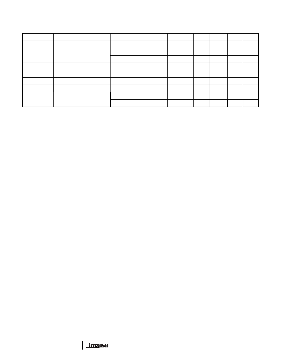
3
I
S
Supply Current (Per Amplifier)
V
S
= ±15V, No Load
25∞C
5.2
7
mA
T
MIN,
T
MAX
7.6
mA
V
S
= ±5V, No Load
25∞C
5.0
mA
R
IN
Input Resistance
Differential
25∞C
150
k
Common-Mode
25∞C
15
M
C
IN
Input Capacitance
A
V
= +1@ 10MHz
25∞C
1.0
pF
R
OUT
Output Resistance
A
V
= +1
25∞C
50
m
PSOR
Power-Supply Operating Range
Dual-Supply
25∞C
±2.0
±18.0
V
Single-Supply
25∞C
2.5
36.0
V
NOTE:
1. Measured from T
MIN
to T
MAX
.
DC Electrical Specifications
V
S
= ±15V, R
L
= 1000
, unless otherwise specified. (Continued)
PARAMETER
DESCRIPTION
CONDITION
TEMP
MIN
TYP
MAX
UNITS
EL2344

4
Closed-Loop AC Electrical Specifications
V
S
= ±15V, A
V
= +1, R
L
= 1000
unless otherwise specified.
PARAMETER
DESCRIPTION
CONDITION
TEMP
MIN
TYP
MAX
UNITS
BW
-3dB Bandwidth (V
OUT
= 0.4V
PP
)
V
S
= ±15V, A
V
= +1
25∞C
120
MHz
V
S
= ±15V, A
V
= -1
25∞C
60
MHz
V
S
= ±15V, A
V
= +2
25∞C
60
MHz
V
S
= ±15V, A
V
= +5
25∞C
12
MHz
V
S
= ±15V, A
V
= +10
25∞C
6
MHz
V
S
= ±5V, A
V
= +1
25∞C
80
MHz
GBWP
Gain-Bandwidth Product
V
S
= ±15V
25∞C
60
MHz
V
S
= ±5V
25∞C
45
MHz
PM
Phase Margin
R
L
= 1k
, C
L
= 10pF
25∞C
50
∞
CS
Channel Separation
f = 5MHz
25∞C
85
dB
SR
Slew Rate (Note 1)
V
S
= ±15V, R
L
= 1000
25∞C
250
325
V/µs
V
S
= ±5V, R
L
= 500
25∞C
200
V/µs
FPBW
Full-Power Bandwidth (Note 2)
V
S
= ±15V
25∞C
4.0
5.2
MHz
V
S
= ±5V
25∞C
12.7
MHz
t
R
, t
F
Rise Time, Fall Time
0.1V Step
25∞C
3.0
ns
OS
Overshoot
0.1V Step
25∞C
20
%
t
PD
Propagation Delay
25∞C
2.5
ns
t
S
Settling to +0.1% (A
V
= +1)
V
S
= ±15V, 10V Step
25∞C
80
ns
V
S
= ±5V, 5V Step
25∞C
60
ns
d
G
Differential Gain (Note 3)
NTSC/PAL
25∞C
0.04
%
d
P
Differential Phase (Note 3)
NTSC/PAL
25∞C
0.15
∞
e
N
Input Noise Voltage
10kHz
25∞C
15.0
nH
/
Hz
i
N
Input Noise Current
10kHz
25∞C
1.50
pA/
Hz
CI STAB
Load Capacitance Stability
A
V
= +1
25∞C
Infinite
pF
NOTES:
1. Slew rate is measured on rising edge.
2. For V
S
= ±15V, V
OUT
= 20V
PP
. For V
S
= ±5V, V
OUT
= 5 V
PP
. Full-power bandwidth is based on slew rate measurement using:
FPBW = SR/(2
* Vpeak).
3. Video Performance measured at V
S
= ±15V, A
V
= +2 with 2 times normal video level across R
L
= 150
. This corresponds to standard video levels
across a back-terminated 75
load. For other values of R
L
, see curves.
EL2344

5
Typical Performance Curves
T
A
= 25∞C, R
L
= 1000
, A
V
= +1 unless otherwise specified.
Non-Inverting
Frequency Response
Inverting Frequency Response
Frequency Response for
Various Load Resistances
Equivalent Input Noise
Output Voltage Swing
vs Frequency
Open-Loop Gain and
Phase vs Frequency
CMRR, PSRR and Closed-Loop
Output Resistance vs Frequency
2nd and 3rd Harmonic
Distortion vs Frequency
Settling Time vs
Output Voltage Change
Output Voltage Range
vs Supply Voltage
Common-Mode Input Range
vs Supply Voltage
Supply Current vs
Supply Voltage
EL2344