 | –≠–ª–µ–∫—Ç—Ä–æ–Ω–Ω—ã–π –∫–æ–º–ø–æ–Ω–µ–Ω—Ç: EL2360CS | –°–∫–∞—á–∞—Ç—å:  PDF PDF  ZIP ZIP |
1
Æ
FN7065
CAUTION: These devices are sensitive to electrostatic discharge; follow proper IC Handling Procedures.
1-888-INTERSIL or 321-724-7143
|
Intersil (and design) is a registered trademark of Intersil Americas Inc.
Copyright © Intersil Americas Inc. 2003. All Rights Reserved. Elantec is a registered trademark of Elantec Semiconductor, Inc.
All other trademarks mentioned are the property of their respective owners.
EL2360
Triple 130MHz Current Feedback Amplifier
The EL2360 is a triple current-
feedback operational amplifier which
achieves a -3dB bandwidth of 130MHz
at a gain of +2. Built using the Elantec proprietary monolithic
complementary bipolar process, these amplifiers use current
mode feedback to achieve more bandwidth at a given gain
than a conventional voltage feedback amplifier.
The EL2360 is designed to drive a double terminated 75
coax cable to video levels. It's fast slew rate of 1500V/µs,
combined with the triple amplifier topology, makes its ideal
for RGB video applications.
This amplifier can operate on any supply voltage from 4V
(±2V) to 33V (±16.5V), yet consume only 8mA per amplifier
at any supply voltage. The EL2360 is available in 16-pin
PDIP and SOIC packages.
For Single, Dual, or Quad applications, consider the EL2160,
EL2260, or EL2460 all in industry standard pin outs. For
Single applications with a power down feature, consider the
EL2166.
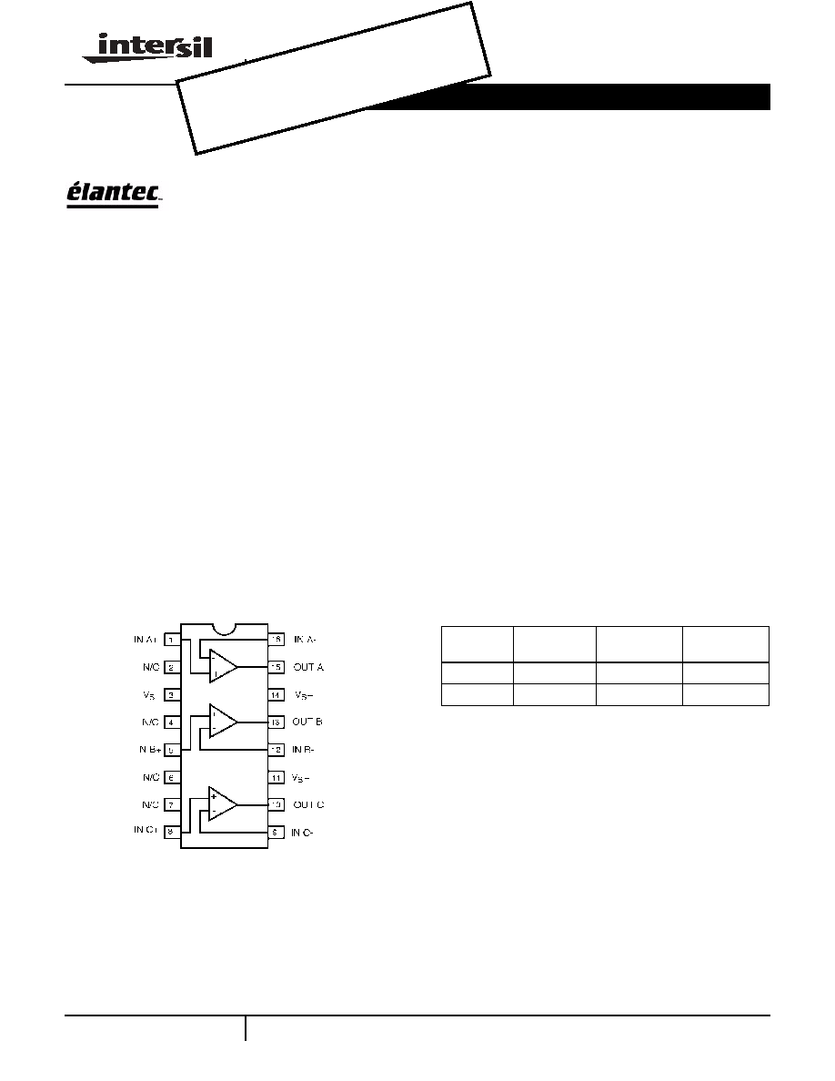
Pinout
Features
∑ Triple amplifier topology
∑ 130MHz -3dB bandwidth (A
V
=+2)
∑ 180MHz -3dB bandwidth (A
V
=+1)
∑ Wide supply range, ±2V to ±15V
∑ 80mA output current (peak)
∑ Low cost
∑ 1500V/µs slew rate
∑ Input common mode range to within 1.5V of supplies
∑ 35ns settling time to 0.1%
∑ Available in single (EL2160), dual (EL2260), and quad
(EL2460) form
Applications
∑ RGB amplifiers
∑ Video amplifiers
∑ Cable driver
∑ Test equipment amplifiers
∑ Current to voltage converters
∑ Video broadcast equipment
EL2360
(16-PIN SO, PDIP)
TOP VIEW
Ordering Information
PART
NUMBER
TEMP. RANGE
PACKAGE
PKG. NO.
EL2360CN
-40∞C to +85∞C
16-Pin PDIP
MDP0031
EL2360CS
-40∞C to +85∞C
16-Pin SOIC
MDP0027
Data Sheet
June 1996, Rev A
OBS
OLE
TE P
ROD
UCT
NO
REC
OMM
END
ED R
EPL
ACE
MEN
T
cont
act o
ur T
echn
ical
Sup
port
Cen
ter a
t
1-88
8-IN
TER
SIL
or w
ww.
inte
rsil.c
om/
tsc

2
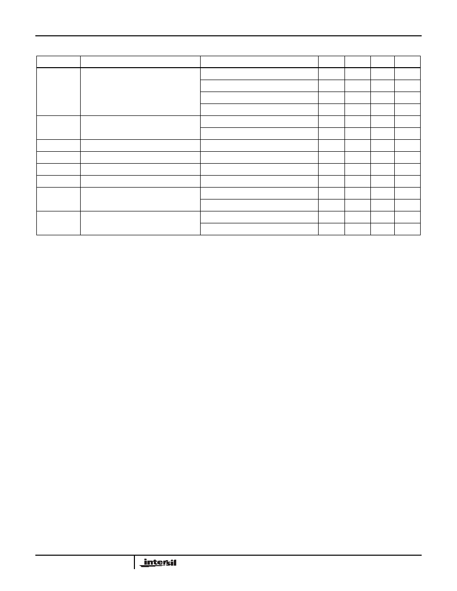
Absolute Maximum Ratings
(T
A
= 25∞C)
Voltage between V
S
+ and V
S
- . . . . . . . . . . . . . . . . . . . . . . . . . .+33V
Common-Mode Input Voltage . . . . . . . . . . . . . . . . . . . . . V
S
- to V
S
+
Differential Input Voltage . . . . . . . . . . . . . . . . . . . . . . . . . . . . . . .±6V
Current into +IN or -IN . . . . . . . . . . . . . . . . . . . . . . . . . . . . . . ±10mA
Internal Power Dissipation . . . . . . . . . . . . . . . . . . . . . . . See Curves
Output Current (continuous) . . . . . . . . . . . . . . . . . . . . . . . . . ±50mA
Operating Ambient Temperature Range . . . . . . . . . . -40∞C to +85∞C
Operating Junction Temperature . . . . . . . . . . . . . . . . . . . . . . . 150∞C
Storage Temperature Range . . . . . . . . . . . . . . . . . . -65∞C to +150∞C
CAUTION: Stresses above those listed in "Absolute Maximum Ratings" may cause permanent damage to the device. This is a stress only rating and operation of the
device at these or any other conditions above those indicated in the operational sections of this specification is not implied.
IMPORTANT NOTE: All parameters having Min/Max specifications are guaranteed. Typical values are for information purposes only. Unless otherwise noted, all tests
are at the specified temperature and are pulsed tests, therefore: T
J
= T
C
= T
A
DC Electrical Specifications
V
S
= ±15V, R
L
=150
, T
A
=25∞C unless otherwise specified.
PARAMETER
DESCRIPTION
CONDITIONS
MIN
TYP
MAX
UNITS
V
OS
Input Offset Voltage
V
S
= ±5V, ±15V
2
10
mV
TCV
OS
Average Input Offset Voltage Drift (Note 1)
10
µV/∞C
+I
IN
+Input Current
V
S
= ±5V, ±15V
0.5
3
µA
-I
IN
-Input Current
V
S
= ±5V, ±15V
5
25
µA
CMRR
Common Mode Rejection Ratio (Note 2)
V
S
= ±5V, ±15V
50
55
dB
-ICMR
-Input Current Common Mode Rejection
(Note 2)
V
S
= ±5V, ±15V
0.2
5
µA/V
PSRR
Power Supply Rejection Ratio (Note 3)
75
95
dB
-IPSR
-Input Current Power Supply Rejection
(Note 3)
0.2
5
µA/V
R
OL
Transimpedance (Note 4)
V
S
= ±15V, R
L
= 400
500
2000
k
V
S
= ±15V, R
L
= 150
500
1800
k
+R
IN
+ Input Resistance
1.5
3
M
+C
IN
+ Input Capacitance
PDIP package
1.5
pF
SOIC package
1
pF
CMIR
Common Mode Input Range
V
S
= ±15V
±13.5
V
V
S
= ±5V
±3.5
V
V
O
Output Voltage Swing
V
S
= ±15V, R
L
= 400
±12
±13.5
V
V
S
= ±15V, R
L
= 150
±12
V
V
S
= ±5V, R
L
= 150
±3.0
±3.7
V
I
SC
Output Short Circuit Current (Note 5)
V
S
= ±5V, ±15V
60
100
150
mA
I
S
Supply Current (per amplifier)
V
S
= ±15V
8.0
11.3
mA
V
S
= ±5V
5.7
8.8
mA
NOTES:
1. Measured from T
MIN
to T
MAX
.
2. V
CM
= ±10V for V
S
= ±15V, V
CM
= ±3V for V
S
= ±5V.
3. The supplies are moved from ±2.5V to ±15V.
4. V
OUT
= ±7V for V
S
= ±15V, V
OUT
= ±2V for V
S
= ±5V.
5. A heat sink is required to keep junction temperature below absolute maximum when an output is shorted.
EL2360
3
NOTES:
1. All AC tests are performed on a "warmed up" part, except Slew Rate, which is pulse tested.
2. Slew Rate is with V
OUT
from +10V to -10V and measured at +5V and -5V.
3. DC offset from -0.714V to +0.714V, AC amplitude 286mV
P-P
, f = 3.58MHz.
AC Electrical Specifications
V
S
= ±15V, A
V
= +2, R
F
=R
G
=560
, R
L
=150
, T
A
=25∞C unless otherwise specified. (Note 1)
PARAMETER
DESCRIPTION
CONDITIONS
MIN
TYP
MAX
UNITS
BW
-3dB Bandwidth
V
S
= ±15V, A
V
= +2
130
MHz
V
S
= ±15V, A
V
= +1
180
MHz
V
S
= ±5V, A
V
= +2
100
MHz
V
S
= ±5V, A
V
= +1
110
MHz
SR
Slew Rate (Note 2)
R
L
= 400
1000
1500
V/µs
R
F
= 1 k
, R
G
= 110
, R
L
= 400
1500
V/µs
t
R
, t
F
Rise Time, Fall Time
V
OUT
= ±500mV
2.7
ns
t
PD
Propagation Delay
V
OUT
= ±500mV
3.2
ns
OS
Overshoot
V
OUT
= ±500mV
0
%
t
S
0.1% Settling Time
V
OUT
= ±2.5V, A
V
= -1
35
ns
dG
Differential Gain (Note 3)
R
L
= 150
0.025
%
R
L
= 500
0.006
%
dP
Differential Phase (Note 3)
R
L
= 150
0.1
∞
R
L
= 500
0.005
∞
EL2360
4
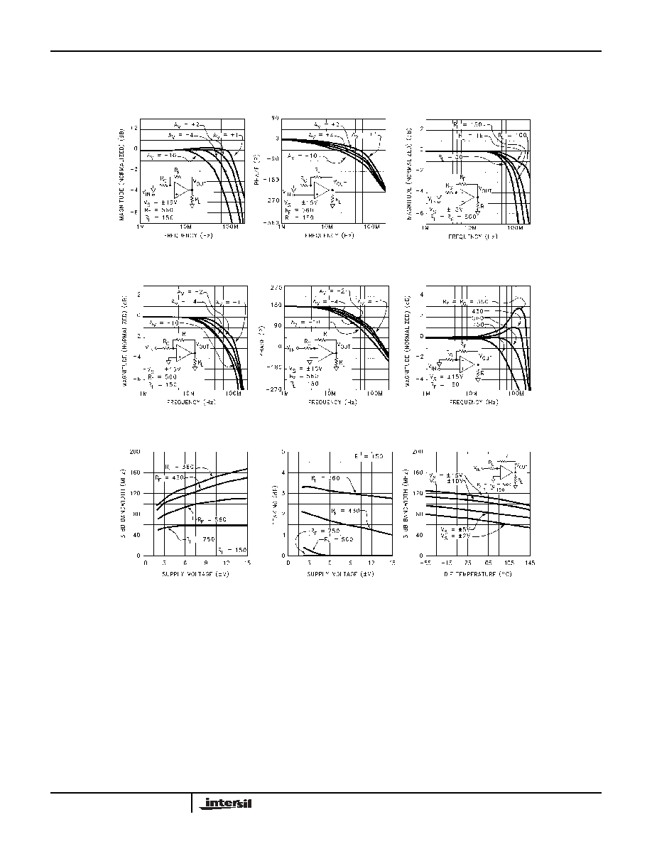
Typical Performance Curves
Non-Inverting Frequency
Response (Gain)
Non-Inverting Frequency
Response (Phase)
Frequency Response
for Various R
L
Inverting Frequency
Response (Gain)
Inverting Frequency
Response (Phase)
Frequency Response for
Various R
F
and R
G
3dB Bandwidth vs Supply
Voltage for A
V
= -1
Peaking vs Supply Voltage
for A
V
= -1
3dB Bandwidth vs
Temperature for A
V
= - 1
EL2360

5
Typical Performance Curves
(Continued)
3dB Bandwidth vs Supply
Voltage for A
V
= +1
Peaking vs Supply Voltage
for A
V
= +1
3dB Bandwidth vs Temperature
for A
V
= +1
3dB Bandwidth vs Supply
Voltage for A
V
= +2
Peaking vs Supply Voltage
for A
V
= +2
3dB Bandwidth vs Temperature
for A
V
= +2
3dB Bandwidth vs Supply
Voltage for A
V
= +10
Peaking vs Supply Voltage
for A
V
= +10
3dB Bandwidth vs Temperature
for A
V
= +10
EL2360