1
Æ
FN7155.1
CAUTION: These devices are sensitive to electrostatic discharge; follow proper IC Handling Procedures.
1-888-INTERSIL or 321-724-7143
|
Intersil (and design) is a registered trademark of Intersil Americas Inc.
Copyright © Intersil Americas Inc. 2004. All Rights Reserved. Elantec is a registered trademark of Elantec Semiconductor, Inc.
All other trademarks mentioned are the property of their respective owners.
Manufactured under U.S. Patent No. 5,418,495
EL2386
250MHz Triple Current Feedback Amplifier
with Disable
The EL2386 is a triple current-
feedback operational amplifier which
achieves a -3dB bandwidth of 250MHz
at a gain of +1 while consuming only 3mA of supply current
per amplifier. It will operate with dual supplies ranging from
±1.5V to ±6V, or from single supplies ranging from +3V to
+12V. The EL2386 also includes a disable/power-down
feature which reduces current consumption to 0mA while
placing the amplifier output in a high impedance state. In
spite of its low supply current, the EL2386 can output 55mA
while swinging to ±4V on ±5V supplies. These attributes
make the EL2386 an excellent choice for low power and/or
low voltage cable-driver, HDSL, or RGB applications.
For single and dual applications, consider the EL2186/
EL2286. For single, dual, and quad applications without
disable, consider the EL2180, EL2280, or EL2480, all in
industry-standard pinouts. The EL2180 also is available in
the tiny SOT-23 package, which is 28% the size of an SO8
package. For lower power applications where speed is still a
concern, consider the EL2170/EL2176 family which also
comes in similar single, dual, and quad configurations. The
EL2170/EL2176 family provides a -3dB bandwidth of 70MHz
while consuming 1mA of supply current per amplifier.
Features
∑ Triple amplifier topology
∑ 3mA supply current (per amplifier)
∑ 250MHz -3dB bandwidth
∑ Low cost
∑ Fast disable
∑ Powers down to 0mA
∑ Single- and dual-supply operation down to ±1.5V
∑ 0.05%/0.05∞ diff. gain/diff. phase into 150
∑ 1200V/µs slew rate
∑ Large output drive current: 55mA
∑ Available in single (EL2186) and dual (EL2286)
∑ Non power-down versions available in single, dual, and
quad (EL2180, EL2280, EL2480)
∑ Lower power EL2170/EL2176 family also available
(1mA/70MHz) in single, dual, and quad
∑ Pb-free available
Applications
∑ Low power/battery applications
∑ HDSL amplifiers
∑ Video amplifiers
∑ Cable drivers
∑ RGB amplifiers
∑ Test equipment amplifiers
∑ Current to voltage converters
∑ Multiplexing
∑ Video broadcast equipment
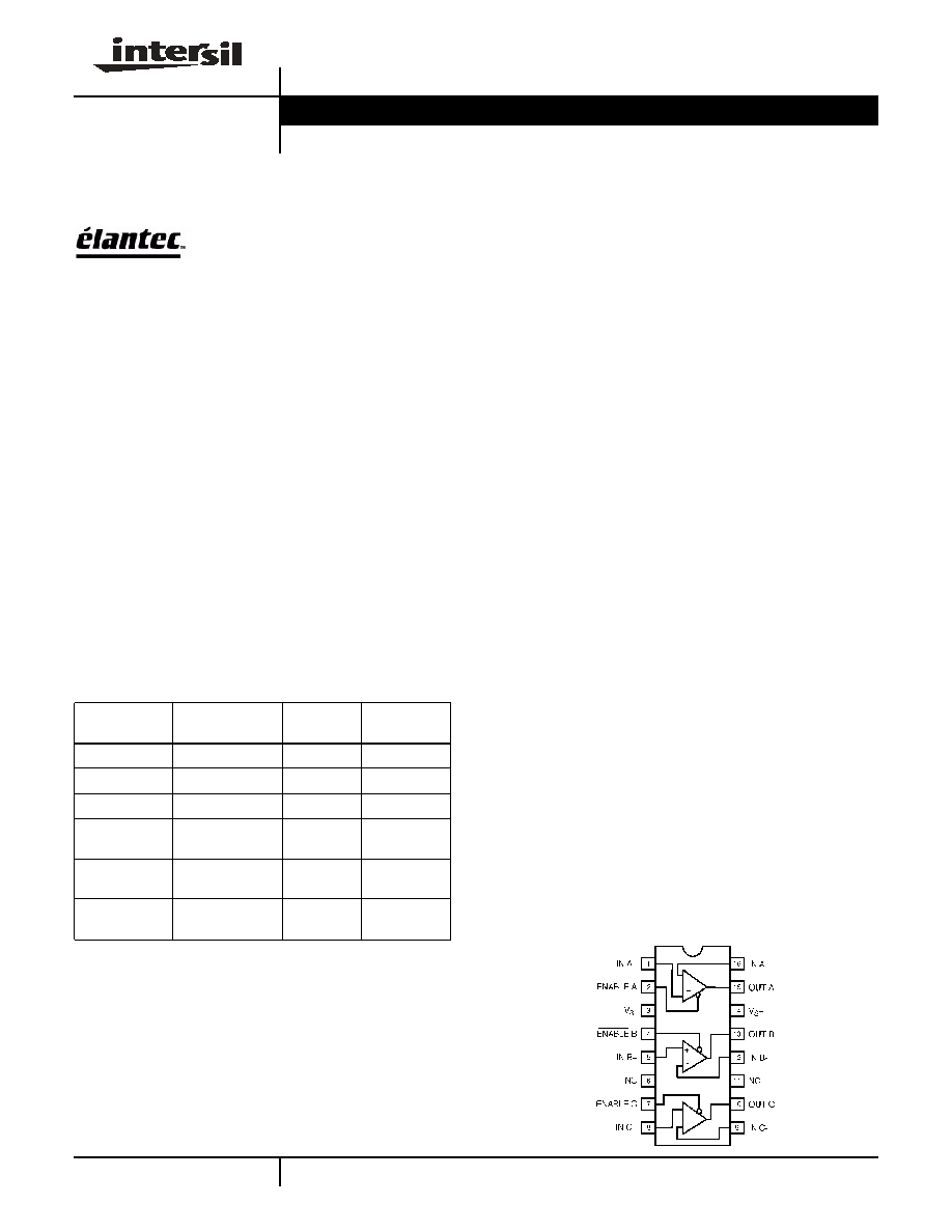
Pinout
EL2386
(16-PIN SO)
TOP VIEW
Ordering Information
PART NUMBER
PACKAGE
TAPE &
REEL
PKG. DWG. #
EL2386CS
16-Pin SO (0.150")
-
MDP0027
EL2386CS-T7
16-Pin SO (0.150")
7"
MDP0027
EL2386CS-T13 16-Pin SO (0.150")
13"
MDP0027
EL2386CSZ
(Note)
16-Pin SO (0.150")
(Pb-Free)
-
MDP0027
EL2386CSZ-T7
(Note)
16-Pin SO (0.150")
(Pb-Free)
7"
MDP0027
EL2386CSZ-
T13 (Note)
16-Pin SO (0.150")
(Pb-Free)
13"
MDP0027
NOTE: Intersil Pb-free products employ special Pb-free material
sets; molding compounds/die attach materials and 100% matte tin
plate termination finish, which is compatible with both SnPb and
Pb-free soldering operations. Intersil Pb-free products are MSL
classified at Pb-free peak reflow temperatures that meet or exceed
the Pb-free requirements of IPC/JEDEC J Std-020B.
Data Sheet
June 24, 2004
2
Absolute Maximum Ratings
(T
A
= 25∞C)
Voltage between V
S
+ and V
S
- . . . . . . . . . . . . . . . . . . . . . . . . +12.6V
Common-Mode Input Voltage . . . . . . . . . . . . . . . . . . . . . V
S
- to V
S
+
Differential Input Voltage . . . . . . . . . . . . . . . . . . . . . . . . . . . . . . .±6V
Current into +IN or -IN . . . . . . . . . . . . . . . . . . . . . . . . . . . . . .±7.5mA
Internal Power Dissipation . . . . . . . . . . . . . . . . . . . . . . . See Curves
Operating Ambient Temperature Range . . . . . . . . . .-40∞C to +85∞C
Operating Junction Temperature . . . . . . . . . . . . . . . . . . . . . . . 150∞C
Output Current . . . . . . . . . . . . . . . . . . . . . . . . . . . . . . . . . . . . ±60mA
CAUTION: Stresses above those listed in "Absolute Maximum Ratings" may cause permanent damage to the device. This is a stress only rating and operation of the
device at these or any other conditions above those indicated in the operational sections of this specification is not implied.
IMPORTANT NOTE: All parameters having Min/Max specifications are guaranteed. Typical values are for information purposes only. Unless otherwise noted, all tests
are at the specified temperature and are pulsed tests, therefore: T
J
= T
C
= T
A
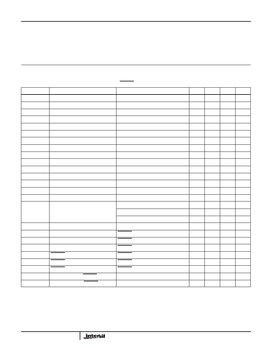
DC Electrical Specifications
V
S
= ±5V, R
L
= 150
, ENABLE = 0V, T
A
= 25∞C unless otherwise specified.
PARAMETER
DESCRIPTION
CONDITIONS
MIN
TYP
MAX
UNIT
V
OS
Input Offset Voltage
2.5
15
mV
TCV
OS
Average Input Offset Voltage Drift
Measured from T
MIN
to T
MAX
5
µV/∞C
dV
OS
V
OS
Matching
0.5
mV
+I
IN
+Input Current
1.5
15
µA
d+I
IN
+I
IN
Matching
20
nA
-I
IN
-Input Current
16
40
µA
d-I
IN
-I
IN
Matching
2
µA
CMRR
Common Mode Rejection Ratio
V
CM
= ±3.5V
45
50
dB
-ICMR
-Input Current Common Mode Rejection V
CM
= ±3.5V
5
30
µA/V
PSRR
Power Supply Rejection Ratio
V
S
= ±4V to ±6V
60
70
dB
-IPSR
-Input Current Power Supply Rejection
V
S
= ±4V to ±6V
1
15
µA/V
R
OL
Transimpedance
V
OUT
= ±2.5V
120
300
k
+R
IN
+Input Resistance
V
CM
= ±3.5V
0.5
2
M
+C
IN
+Input Capacitance
1.2
pF
CMIR
Common Mode Input Range
±3.5
±4.0
V
V
O
Output Voltage Swing
V
S
= ±5V
±3.5
±4.0
V
V
S
= +5V single-supply, high
4.0
V
V
S
= +5V single-supply, low
0.3
V
I
O
Output Current
50
55
mA
I
S
Supply Current - Enabled (per amplifier)
ENABLE = 2.0V
3
6
mA
I
S(DIS)
Supply Current - Disabled (per amplifier) ENABLE = 4.5V
0
50
µA
C
OUT(DIS)
Output Capacitance - Disabled
ENABLE = 4.5V
4.4
pF
R
IN-EN
ENABLE Pin Input Resistance
ENABLE = 2.0V to 4.5V
45
85
k
I
IH-EN
ENABLE Pin Input Current - High
ENABLE = 4.5V
-0.04
µA
I
IL-EN
ENABLE Pin Input Current - Low
ENABLE = 0V
-53
µA
V
DIS
Minimum Voltage at ENABLE to Disable
4.5
V
V
EN
Maximum Voltage at ENABLE to Enable
2.0
V
EL2386

3
AC Electrical Specifications
V
S
= ±5V, R
F
= R
G
= 750
, R
L
= 150W, ENABLE = 0V, T
A
= 25∞C unless otherwise specified.
PARAMETER
DESCRIPTION
CONDITIONS
MIN
TYP
MAX
UNIT
BW
-3dB Bandwidth
A
V
= +1
250
MHz
A
V
= +2
180
MHz
BW
±0.1dB Bandwidth
A
V
= +2
50
MHz
SR
Slew Rate
V
OUT
= ±2.5V, measured at ±1.25V
600
1200
V/µs
t
R
, t
F
Rise and Fall Time
V
OUT
= ±500mV
1.5
ns
t
PD
Propagation Delay
V
OUT
= ±500mV
1.5
ns
OS
Overshoot
V
OUT
= ±500mV
3.0
%
t
S
0.1% Settling
V
OUT
= ±2.5V, A
V
= -1
15
ns
d
G
Differential Gain (Note 1)
A
V
= +2, R
L
= 150
0.05
%
d
P
Differential Phase (Note 1)
A
V
= +2, R
L
= 150
0.05
∞
d
G
Differential Gain (Note 1)
A
V
= +1, R
L
= 500
0.01
%
d
P
Differential Phase (Note 1)
A
V
= +1, R
L
= 500
0.01
∞
t
ON
Turn-On Time (Note 2)
A
V
= +2, V
IN
= +1V, R
L
= 150
40
100
ns
t
OFF
Turn-Off Time (Note 2)
A
V
= +2, V
IN
= +1V, R
L
= 150
800
2000
ns
C
S
Channel Separation
f = 5MHz
85
dB
NOTES:
1. DC offset from 0V to 0.714V, AC amplitude 286mV
P-P
, f = 3.58MHz.
2. Measured from the application of the logic signal until the output voltage is at the 50% point between initial and final values.
EL2386
4
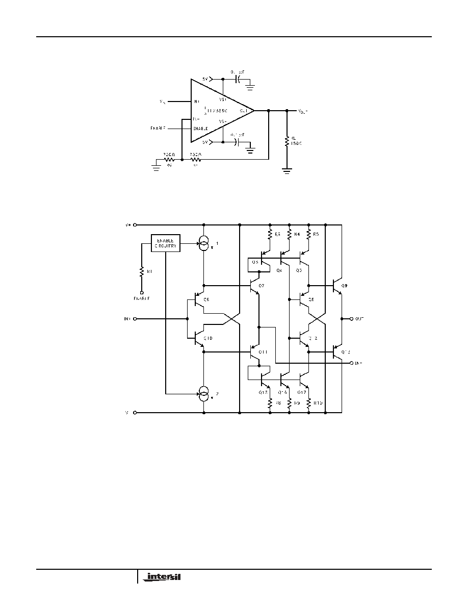
Test Circuit
(per Amplifier)
Simplified Schematic
(per Amplifier)
EL2386

5
Typical Performance Curves
NON-INVERTING REQUENCY
RESPONSE (GAIN)
NON-INVERTING FREQUENCY
RESPONSE (PHASE)
FREQUENCY RESPONSE
FOR VARIOUS R
F
AND R
G
INVERTING FREQUENCY
RESPONSE (GAIN)
INVERTING FREQUENCY
RESPONSE (PHASE)
FREQUENCY RESPONSE
FOR VARIOUS R
L
AND C
L
TRANSIMPEDANCE (R
OL
)
vs FREQUENCY
PSRR AND CMRR vs
FREQUENCY
FREQUENCY RESPONSE
FOR VARIOUS C
IN
-
EL2386