 | –≠–ª–µ–∫—Ç—Ä–æ–Ω–Ω—ã–π –∫–æ–º–ø–æ–Ω–µ–Ω—Ç: EL4094CS | –°–∫–∞—á–∞—Ç—å:  PDF PDF  ZIP ZIP |
1
Æ
FN7160
CAUTION: These devices are sensitive to electrostatic discharge; follow proper IC Handling Procedures.
1-888-INTERSIL or 321-724-7143
|
Intersil (and design) is a registered trademark of Intersil Americas Inc.
Copyright © Intersil Americas Inc. 2003. All Rights Reserved. Elantec is a registered trademark of Elantec Semiconductor, Inc.
All other trademarks mentioned are the property of their respective owners.
EL4094
Video Gain Control/Fader
The EL4094 is a complete two-input
fader. It combines two inputs according
to the equation:
V
OUT
= V
INA
(0.5V + V
G
) + V
INB
(0.5V - V
G
),
where V
GAIN
is the difference between V
GAIN
and V
GAIN
pin voltages and ranges from -0.5V to +0.5V. It has a wide
60MHz bandwidth at -3dB, and is designed for excellent
video distortion performance. The EL4094 is the same circuit
as the EL4095, but with feedback resistors included on-chip
to implement unity-gain connection. An output buffer is
included in both circuits.
The gain-control input is also very fast, with a 20MHz small-
signal bandwidth and 70ns recovery time from overdrive.
The EL4094 is compatible with power supplies from ±5V to
±15V, and is available in both the 8-pin plastic DIP and
SO-8.
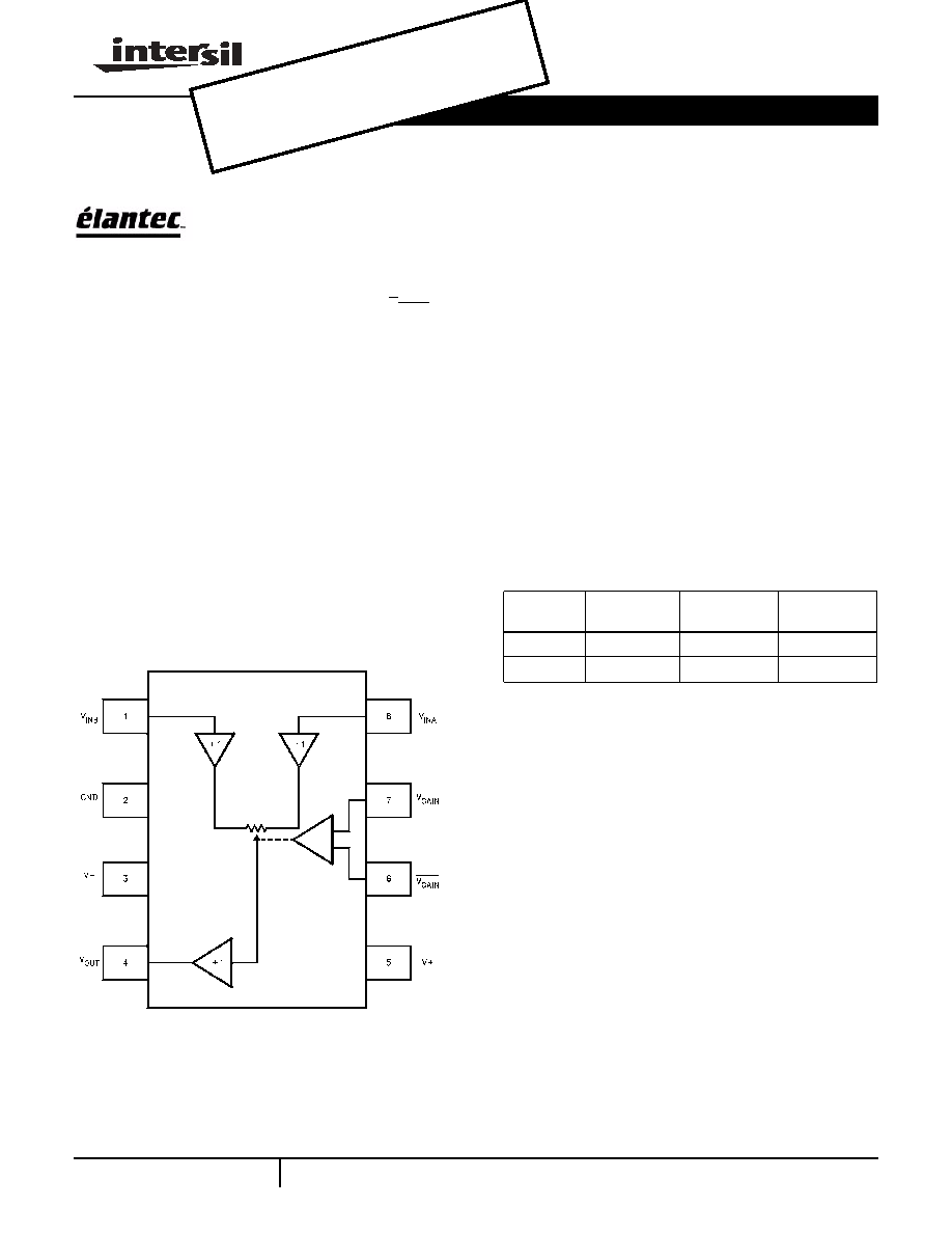
Pinout
Features
∑ Complete video fader
∑ 0.02%/0.04∞ differential gain/phase @100% gain
∑ Output amplifier included
∑ Calibrated linear gain control
∑ ±5V to ±15V operation
∑ 60MHz bandwidth
∑ Low thermal errors
Applications
∑ Video faders/wipers
∑ Gain control
∑ Video text insertion
∑ Level adjust
∑ Modulation
Manufactured under U.S. Patent No. 5,321,371, 5,374,898
EL4094
(8-PIN PDIP, SO)
TOP VIEW
Ordering Information
PART
NUMBER
TEMP. RANGE
PACKAGE
PKG. NO.
EL4094CN
-40∞C to +85∞C
8-Pin PDIP
MDP0031
EL4094CS
-40∞C to +85∞C
8-Pin SO
MDP0027
Data Sheet
August 1996, Rev D
OBS
OLE
TE P
ROD
UCT
NO
REC
OMM
END
ED R
EPL
ACE
MEN
T
con
tact
our
Tec
hnic
al S
upp
ort C
ente
r at
1-88
8-IN
TER
SIL
or w
ww.
inte
rsil.c
om/
tsc

2
Absolute Maximum Ratings
(T
A
= 25∞C)
V
S
+
Voltage between V
S
+ and GND . . . . . . . . . . . . . . . . .+18V
V
S
Voltage between V
S
+ and V
S
- . . . . . . . . . . . . . . . . . .+33V
V
INA
,
Input Voltage . . . . . . . . . . . . . . . . . . . . . . . . . . . (V
S
-) -0.3V
V
INB
to (V
S
+) +0.3V
V
GAIN
Input Voltage . . . . . . . . . . . . . . . . . . . . . . . . . . . V
GAIN
±5V
V
GAIN
Input Voltage . . . . . . . . . . . . . . . . . . . . . . . . . . . V
S
- to V
S
+
I
OUT
Output Current . . . . . . . . . . . . . . . . . . . . . . . . . . . . ±35mA
Internal Power Dissipation. . . . . . . . . . . . . . . . See Curves
T
A
Operating Ambient Temp. Range . . . . . . . . -40∞C to +85∞C
T
J
Operating Junction Temperature . . . . . . . . . . . . . . . . 150∞C
T
ST
Storage Temperature Range . . . . . . . . . . . -65∞C to +150∞C
CAUTION: Stresses above those listed in "Absolute Maximum Ratings" may cause permanent damage to the device. This is a stress only rating and operation of the
device at these or any other conditions above those indicated in the operational sections of this specification is not implied.
IMPORTANT NOTE: All parameters having Min/Max specifications are guaranteed. Typical values are for information purposes only. Unless otherwise noted, all tests
are at the specified temperature and are pulsed tests, therefore: T
J
= T
C
= T
A
Open-Loop DC Electrical Specifications
V
S
= ±5V, T
A
= 25∞C, V
GAIN
= +0.6V to measure channel A, V
GAIN
= -0.6V to
measure channel B, V
GAIN
= 0V, unless otherwise specified. NL, A
V
= 0.25V
PARAMETER
DESCRIPTION
LIMITS
UNITS
MIN
TYP
MAX
V
OS
Input Offset Voltage
4
30
mV
I
B
+
V
IN
Input Bias Current
2
10
µA
PSRR
Power Supply Rejection Ratio
60
80
dB
EG
Gain Error, 100% Setting
-0.5
-0.8
%
V
IN
V
IN
Range
(V-) +2.5
(V+) -2.5
V
V
O
Output Voltage Swing
(V-) +2.5
(V+) -2.5
V
I
SC
Output Short-Circuit Current
50
95
150
mA
V
GAIN
, 100%
Minimum Voltage at V
GAIN
for 100% Gain
0.45
0.5
0.55
V
V
GAIN
, 0%
Maximum Voltage at V
GAIN
for 0% Gain
-0.55
-0.5
-0.45
V
NL, Gain
Gain Control Non-linearity, V
IN
= ±0.5V
1.5
4
%
NL, A
V
= 1
Signal Non-linearity, V
IN
= 0 to ±1V, V
GAIN
= 0.55V
0.01
%
A
V
= 0.5
Signal Non-linearity, V
IN
= 0 to ±1V, V
GAIN
= 0V
0.05
%
A
V
= 0.25
Signal Non-linearity, V
IN
= 0 to ±1V, V
GAIN
= -0.25V
0.2
0.5
%
R
GAIN
Resistance between V
GAIN
and V
GAIN
4.6
5.5
6.6
k
I
S
Supply Current
12
14.5
19
mA
F
T
Off-Channel Feedthrough
-75
-50
dB
Closed-Loop AC Electrical Specifications
V
S
= ±15V, C
L
= 15pF, T
A
= 25∞C, A
V
= 100% unless otherwise noted.
PARAMETER
DESCRIPTION
LIMITS
UNITS
MIN
TYP
MAX
SR
Slew Rate; V
OUT
from -3V to +3V measured at -2V and +2V
370
500
V/µs
BW
Bandwidth,
-3dB
45
60
MHz
-1dB
35
MHz
-0.1dB
6
MHz
EL4094
3
Typical Performance Curves
dG
Differential Gain, AC amplitude of 286mV
P-P
at 3.58MHz on DC offset of -0.7, 0, and +0.7V
A
V
= 100%
0.02
%
A
V
= 50%
0.20
%
A
V
= 25%
0.40
%
d
Differential Phase, AC amplitude of 286mV
P-P
at 3.58MHz on DC offset of -0.7, 0, and +0.7V
A
V
= 100%
0.04
(∞)
A
V
= 50%
0.20
(∞)
A
V
= 25%
0.20
(∞)
BW, GAIN
-3dB Gain Control Bandwidth, V
GAIN
Amplitude 0.5 V
P-P
20
MHz
T
REC
, GAIN
Gain Control Recovery from Overload; V
GAIN
from -0.6V to 0V
70
ns
Closed-Loop AC Electrical Specifications
V
S
= ±15V, C
L
= 15pF, T
A
= 25∞C, A
V
= 100% unless otherwise noted. (Continued)
PARAMETER
DESCRIPTION
LIMITS
UNITS
MIN
TYP
MAX
Small-Signal Step
Response for Gain = 100%, 50%,
25%, and 0%. V
S
±5V
Large-Signal Step
Response for Gain = 100%, 50%,
25%, and 0%. V
S
±12V
EL4094

4
Typical Performance Curves
(Continued)
Frequency Response vs
Capacitive Loading
Frequency Response vs
Resistive Loading
Frequency Response vs Gain
Off-Channel Isolation
Over Frequency
Output Noise Over Frequency
Change in Slewrate and
Bandwidth with Supply Voltage
EL4094
5
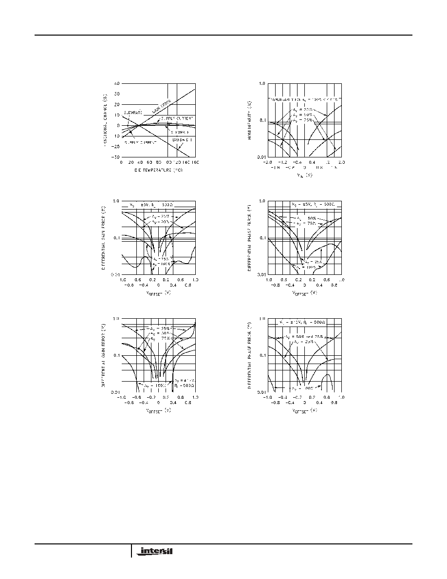
Typical Performance Curves
(Continued)
Change in 100% Gain Error,
Supply Current, Slewrate and
Bandwidth over Temperature
Nonlinearity vs V
IN
for
Gain = 100%, 75%, 50% and 25%
Differential Gain Error vs
V
OFFSET
for Gain = 100%,
75%, 50% and 25%. F = 3.58MHz
Differential Phase Error vs
V
OFFSET
for Gain = 100%,
75%, 50% and 25%. F = 3.58MHz
Differential Gain Error vs
V
OFFSET
for Gain = 100%,
75%, 50% and 25%. F = 3.58MHz
Differential Phase Error vs
V
OFFSET
for Gain = 100%,
75%, 50% and 25%. F = 3.58MHz
EL4094