 | –≠–ª–µ–∫—Ç—Ä–æ–Ω–Ω—ã–π –∫–æ–º–ø–æ–Ω–µ–Ω—Ç: EL4095CS | –°–∫–∞—á–∞—Ç—å:  PDF PDF  ZIP ZIP |
1
Æ
FN7161
CAUTION: These devices are sensitive to electrostatic discharge; follow proper IC Handling Procedures.
1-888-INTERSIL or 321-724-7143
|
Intersil (and design) is a registered trademark of Intersil Americas Inc.
Copyright © Intersil Americas Inc. 2003. All Rights Reserved. Elantec is a registered trademark of Elantec Semiconductor, Inc.
All other trademarks mentioned are the property of their respective owners.
EL4095
Video Gain Control/Fader/Multiplexer
The EL4095 is a versatile variable-gain
building block. At its core is a fader
which can variably blend two inputs
together and an output amplifier that can drive heavy loads.
Each input appears as the input of a current-feedback
amplifier and with external resistors can separately provide
any gain desired. The output is defined as:
V
OUT
= A*V
INA
(0. 5V + V
GAIN
) + B*V
INB
(0.5V≠V
GAIN
),
where A and B are the fed-back gains of each channel.
Additionally, two logic inputs are provided which each
override the analog V
GAIN
control and force 100% gain for
one input and 0% for the other. The logic inputs switch in
only 25ns and provide high attenuation to the off channel,
while generating very small glitches.
Signal bandwidth is 60MHz, and gain-control bandwidth
20MHz. The gain control recovers from overdrive in only
70ns.
The EL4095 operates from ±5V to ±15V power supplies, and
is available in both 14-pin DIP and narrow surface mount
packages.
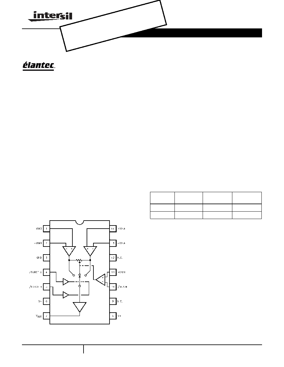
Pinout
Features
∑ Full function video fader
∑ 0.02%/0.02∞ differential gain/phase @ 100% gain
∑ 25ns multiplexer included
∑ Output amplifier included
∑ Calibrated linear gain control
∑ ±5V to ±15V operation
∑ 60MHz bandwidth
∑ Low thermal errors
Applications
∑ Video faders/wipers
∑ Gain control
∑ Graphics overlay
∑ Video text insertion
∑ Level adjust
∑ Modulation
Manufactured under U.S. Patent No. 5,321,371, 5,374,898
EL4095
(14-PIN PDIP, SO)
TOP VIEW
Ordering Information
PART
NUMBER
TEMP. RANGE
PACKAGE
PKG. NO.
EL4095CN
-40∞C to +85∞C
14-Pin PDIP
MDP0031
EL4095CS
-40∞C to +85∞C
14-Pin SO
MDP0027
Data Sheet
August 1996, Rev D
OBS
OLE
TE P
ROD
UCT
NO R
ECO
MME
NDE
D RE
PLA
CEM
ENT
cont
act o
ur T
echn
ical
Sup
port
Cen
ter a
t
1-88
8-IN
TER
SIL
or w
ww.
inte
rsil.c
om/t
sc

2
Absolute Maximum Ratings
(T
A
= 25∞C)
V
S
+
Supply Voltage . . . . . . . . . . . . . . . . . . . . . . . . . . . . . . . .+18V
V
S
Voltage between V
S
+ and V
S
- . . . . . . . . . . . . . . . . . . . .+33V
+V
INA
,Input Voltage . . . . . . . . . . . . . . . . . . . . . . . . . . . . . (V
S
-) -0.3V
+V
INB
. . . . . . . . . . . . . . . . . . . . . . . . . . . . . . . . . . . . to (V
S
+) +0.3V
I
IN
Current Into -V
INA
, -V
INB
. . . . . . . . . . . . . . . . . . . . . . . . 5mA
V
GAIN
Input Voltage . . . . . . . . . . . . . . . . . . . . . . . . . . . . . V
GAIN
±5V
V
GAIN
Input Voltage . . . . . . . . . . . . . . . . . . . . . . . . . . . . . V
S
- to V
S
+
V
FORCE
Input Voltage . . . . . . . . . . . . . . . . . . . . . . . . . . . -1V to +6V
I
OUT
Output Current . . . . . . . . . . . . . . . . . . . . . . . . . . . . . . ±35mA
T
A
Operating Temperature Range . . . . . . . . . . . . -40∞C to +85∞C
T
J
Operating Junction Temperature. . . . . . . . . . . 0∞C to +150∞C
T
ST
Storage Temperature Range. . . . . . . . . . . . . -65∞C to +150∞C
Internal Power Dissipation . . . . . . . . . . . . . . . . . See Curves
CAUTION: Stresses above those listed in "Absolute Maximum Ratings" may cause permanent damage to the device. This is a stress only rating and operation of the
device at these or any other conditions above those indicated in the operational sections of this specification is not implied.
IMPORTANT NOTE: All parameters having Min/Max specifications are guaranteed. Typical values are for information purposes only. Unless otherwise noted, all tests
are at the specified temperature and are pulsed tests, therefore: T
J
= T
C
= T
A
Open-Loop DC Electrical Specifications
V
S
= ±15V, T
A
= 25∞C, V
GAIN
ground unless otherwise specified
PARAMETER
DESCRIPTION
LIMITS
UNITS
MIN
TYP
MAX
V
OS
Input Offset Voltage
1.5
5
mV
I
B
+
+V
IN
Input Bias Current
5
10
µA
I
B
-
-V
IN
Input Bias Current
10
50
µA
CMRR
Common Mode Rejection
65
80
dB
-CMRR
-V
IN
Input Bias Current Common Mode Rejection
0.5
1.5
µA/V
PSRR
Power Supply Rejection Ratio
65
95
dB
-IPSR
-V
IN
Input Current Power Supply Rejection Ratio
0.2
2
µA/V
R
OL
Transimpedance
0.2
0.4
M
R
IN-
-V
IN
Input Resistance
80
V
IN
+V
IN
Range
(V-) + 3.5
(V+) -3.5
V
V
O
Output Voltage Swing
(V-) +2
(V+) -2
V
I
SC
Output Short-Circuit Current
80
125
160
mA
V
IH
Input High Threshold at Force A or Force B Inputs
2.0
V
V
IL
Input Low Threshold at Force A or Force B Inputs
0.8
V
I
FORCE
, High
Input Current of Force A or Force B, V
FORCE
= 5V
-50
µA
I
FORCE
, Low
Input Current of Force A or Force B, V
FORCE
= 0V
-440
-650
µA
Feedthrough,
Forced
Feedthrough of Deselected Input to Output,
Deselected Input at 100% Gain Control
60
75
dB
V
GAIN
, 100%
Minimum Voltage at V
GAIN
for 100% Gain
0.45
0.5
0.55
V
V
GAIN
, 0%
Maximum Voltage at V
GAIN
for 0% Gain
-0.55
-0.5
-0.45
V
NL, Gain
Gain Control Non-linearity, V
IN
= ±0.5V
2
4
%
R
IN
, VG
Impedance between V
GAIN
and V
GAIN
4.5
5.5
6.5
k
NL, A
V
= 1
A
V
= 0.5
A
V
= 0.25
Signal Non-linearity, V
IN
= ±1V, V
GAIN
= 0.55V
Signal Non-linearity, V
IN
= ±1V, V
GAIN
= 0V
Signal Non-linearity, V
IN
= ±1V, V
GAIN
= -0.25V
<0.01
0.03
0.07
0.4
%
%
%
I
S
Supply Current
17
21
mA
EL4095

3
Closed-Loop AC Electrical Specifications
V
S
= ±15V, A
V
= +1, R
F
= R
IN
= 1k
, R
L
= 500
, C
L
= 15pF, C
IN
- = 2pF, T
A
= 25∞C,
A
V
= 100% unless otherwise noted
PARAMETER
DESCRIPTION
LIMITS
UNITS
MIN
TYP
MAX
SR
Slew Rate; V
OUT
from -3V to +3V
Measured at -2V and +2V
330
V/µs
BW
Bandwidth
-3dB
60
MHz
-1dB
30
MHz
-0.1dB
6
MHz
dG
Differential Gain; AC Amplitude of 286mV
P-P
at 3.58MHz
on DC Offset of -0.7V, 0V and +0.7V
A
V
= 100%
0.02
%
A
V
= 50%
0.07
%
A
V
= 25%
0.07
%
d
Differential Phase; AC Amplitude of 286mV
P-P
at
3.58MHz on DC Offset of -0.7V, 0V and +0.7V
A
V
= 100%
0.02
∞
A
V
= 50%
0.05
∞
A
V
= 25%
0.15
∞
T
S
Settling Time to 0.2%; V
OUT
from -2V to +2V
A
V
= 100%
100
ns
A
V
= 25%
100
ns
T
FORCE
Propagation Delay from V
FORCE
= 1.4V to 50%
Output Signal Enabled or Disabled Amplitude
25
ns
BW, Gain
-3dB Gain Control Bandwidth,
V
GAIN
Amplitude 0.5 V
P-P
20
MHz
T
REC
, Gain
Gain Control Recovery from Overload; V
GAIN
from -0.7V
to 0V
70
ns
EL4095

4
Typical Performance Curves
Large-Signal Pulse
Response Gain = +1
Large-Signal Pulse
Response Gain = -1
Small-Signal Pulse Response
for Various Gains
Frequency Response for Different
Gains-A
V
= +1
Frequency Response with Different
Values of R
F
- Gain = +1
Frequency Response with Different
Values of R
F
- Gain = -1
EL4095

5
Typical Performance Curves
(Continued)
Frequency Response with Different
Values of R
F
- Gain = -1
Frequency Response with Various
Load Capacitances and Resistances
Input Noise Voltage and
Current vs Frequency
Frequency Response with Various
Values of Parasitic C
IN
-
Change in Bandwidth and Slewrate with
Supply Voltage - Gain = +1
Change in Bandwidth and Slewrate with
Supply Voltage - Gain = -1
EL4095