1
Æ
FN7163.2
CAUTION: These devices are sensitive to electrostatic discharge; follow proper IC Handling Procedures.
1-888-INTERSIL or 321-724-7143
|
Intersil (and design) is a registered trademark of Intersil Americas Inc.
Copyright © Intersil Americas Inc. 2002-2004. All Rights Reserved. Elantec is a registered trademark of Elantec Semiconductor, Inc.
All other trademarks mentioned are the property of their respective owners
.
EL4332
Triple 2:1 300MHz Mux-Amp A
V
= 2
The EL4332 is a triple very high speed 2:1 Multiplexer-
Amplifier. It is intended primarily for component video
multiplexing and is especially suited for pixel switching. The
amplifiers have their gain set to 2 internally, which reduces
the need for many external components. The gain-of-2
facilitates driving back terminated cables. All three amplifiers
are switched simultaneously from their A to B inputs by the
TTL/CMOS compatible, common A/B control pin.
A -3dB bandwidth of 300MHz together with 3ns multiplexing
time enable the full performance of the fastest component
video systems to be realized.
The EL4332 runs from standard ±5V supplies, and is
available in the narrow 16-pin small outline package.
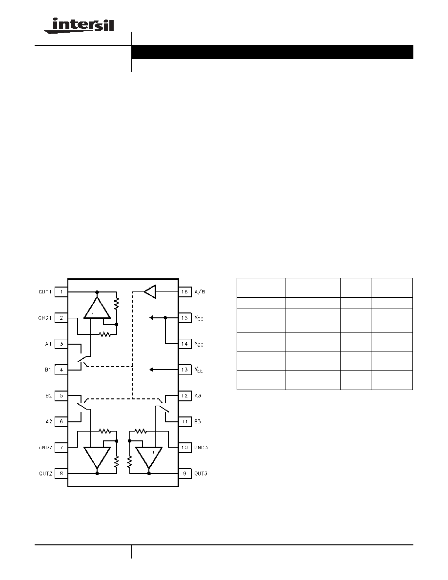
Pinout
Features
∑ 3ns A-B switching
∑ 300MHz bandwidth
∑ Fixed gain of 2, for cable driving
∑ > 650V/µs slew rate
∑ TTL/CMOS compatible switch
∑ Pb-free available
Applications
∑ RGB multiplexing
∑ Picture-in-picture
∑ Cable driving
∑ HDTV processing
∑ Switched gain amplifiers
∑ ADC input multiplexer
Demo Board
A demo PCB is available for this product.
EL4332
[16-PIN SO (0.150")]
TOP VIEW
Ordering Information
PART NUMBER
PACKAGE
TAPE &
REEL
PKG. DWG. #
EL4332CS
16-Pin SO (0.150")
-
MDP0027
EL4332CS-T7
16-Pin SO (0.150")
7"
MDP0027
EL4332CS-T13
16-Pin SO (0.150")
13"
MDP0027
EL4332CSZ
(Note)
16-Pin SO (0.150")
(Pb-Free)
-
MDP0027
EL4332CSZ-T7
(Note)
16-Pin SO (0.150")
(Pb-Free)
7"
MDP0027
EL4332CSZ-T13
(Note)
16-Pin SO (0.150")
(Pb-Free)
13"
MDP0027
NOTE: Intersil Pb-free products employ special Pb-free material
sets; molding compounds/die attach materials and 100% matte tin
plate termination finish, which is compatible with both SnPb and
Pb-free soldering operations. Intersil Pb-free products are MSL
classified at Pb-free peak reflow temperatures that meet or exceed
the Pb-free requirements of IPC/JEDEC J Std-020B.
Data Sheet
October 4, 2004
2
NOTES:
1. Each channel's A-input to its B-input.
2. There is no short circuit protection on any output.
Absolute Maximum Ratings
(T
A
= 25∞C)
V
CC
to V
EE
. . . . . . . . . . . . . . . . . . . . . . . . . . . . . . . . . . . . . . . . .14V
V
CC
to any GND . . . . . . . . . . . . . . . . . . . . . . . . . . . . . . . . . . . . .12V
V
EE
to any GND . . . . . . . . . . . . . . . . . . . . . . . . . . . . . . . . . . . . .12V
Continuous Output Current . . . . . . . . . . . . . . . . . . . . . . . . . . . 45mA
Any Input . . . . . . . . . . . . . . . . . . . . . . . . . . V
EE
-0.3V to V
CC
+0.3V
Input Current, Any Input. . . . . . . . . . . . . . . . . . . . . . . . . . . . . . . 5mA
Power Dissipation . . . . . . . . . . . . . . . . . . . . . . . . . . . . . See Curves
Ambient Operating Temperature . . . . . . . . . . . . . . . . . -40∞C to 85∞C
Junction Temperature . . . . . . . . . . . . . . . . . . . . . . . . . . . . . . . 150∞C
Storage Temperature. . . . . . . . . . . . . . . . . . . . . . . .-60∞C to +150∞C
CAUTION: Stresses above those listed in "Absolute Maximum Ratings" may cause permanent damage to the device. This is a stress only rating and operation of the
device at these or any other conditions above those indicated in the operational sections of this specification is not implied.
IMPORTANT NOTE: All parameters having Min/Max specifications are guaranteed. Typical values are for information purposes only. Unless otherwise noted, all tests
are at the specified temperature and are pulsed tests, therefore: T
J
= T
C
= T
A
DC Electrical Specifications
V
CC
= +5V, V
EE
= -5V, Temperature = 25∞C, R
L
=
PARAMETER
DESCRIPTION
MIN
TYP
MAX
UNITS
V
OS
Input Referred Offset Voltage
8
20
mV
dV
OS
Input Referred Offset Voltage Delta (Note 1)
2
8
mV
R
IN
Input Resistance
30
k
I
B
Input Bias Current
-7
-30
µA
dI
B
Input Bias Current Delta (Note 1)
0.5
4.0
µA
A
V
Gain
1.94
2.00
2.06
V/V
dA
V
Gain Delta (Note 1)
0.5
2.5
%
C
IN
Input Capacitance
3.3
pF
PSRR
Power Supply Rejection Ratio
50
70
dB
V
O
Output Voltage Swing into 500
load
±2.7
±3.6
V
Output Voltage Swing into 150
load
+3/-2.7
V
I
OUT
Current Output, Measured with 75
Load (Note 2)
30
40
mA
Xtalk
AB
Crosstalk from Non-selected Input (at DC)
-70
-100
dB
Xtalk
CH-CH
Crosstalk from one Amplifier to another Amplifier
-70
-100
dB
V
IH
Input Logic High Level
2.0
V
V
IL
Input Logic Low Level
0.8
V
I
IL
Logic Low Input Current (V
IN
= 0V)
-0.3
-40
-80
µA
I
IH
Logic High Input Current (V
IN
= 0V)
-3
0
3
µA
I
S
Total Supply Current
38
48
60
mA
AC Electrical Specifications
V
CC
= +5V, V
EE
= -5V, Temperature = 25∞C, R
L
= 150
, C
L
= 3pF.
PARAMETER
DESCRIPTION
MIN
TYP
MAX
UNITS
BW
-3dB Bandwidth
300
MHz
BW 0.1dB
±0.1dB Bandwidth
105
MHz
DG
Differential Gain at 3.58MHz
0.04
%
DP
Differential Phase at 3.58MHz
0.08
∞
Pkg
Peaking with Nominal Load
0.2
dB
SR
Slew Rate (4V Square Wave, Measured 25%≠75%)
650
V/µs
EL4332

3
Burn In Schematic
t
S
Settling Time to 0.1% of Final Value
13
ns
T
SW
Time to Switch Inputs
3
ns
OS
Overshoot, V
OUT
= 4V
P-P
8
%
I
SO
ab
10M
Input to Input Isolation at 10MHz
60
dB
100M
Input to Input Isolation at 100MHz
40
dB
I
SO
ch-ch
10M
Channel to Channel Isolation at 10MHz
61
dB
100M
Channel to Channel Isolation at 100MHz
50
dB
AC Electrical Specifications
V
CC
= +5V, V
EE
= -5V, Temperature = 25∞C, R
L
= 150
, C
L
= 3pF. (Continued)
PARAMETER
DESCRIPTION
MIN
TYP
MAX
UNITS
Pin Descriptions
PIN NAME
FUNCTION
A1, A2, A3
"A" inputs to amplifiers 1, 2 and 3 respectively.
B1, B2, B3
"B" inputs to amplifiers 1, 2 and 3 respectively.
GND1, GND2, GND3
These are the individual ground pins for each channel.
Out1, Out2, Out3
Amplifier outputs. Note: there is no short circuit protection on any output.
V
CC
Positive power supply. Typically +5V.
V
EE
Negative power supply. Typically -5V.
A/B
Common input select pin, a logic high selects the "A" inputs, logic low selects the "B" inputs. CMOS/TTL
compatible.
EL4332
4
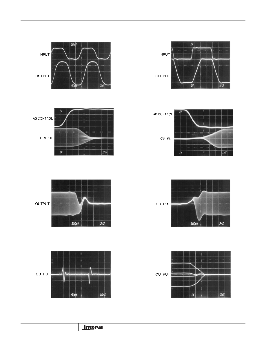
Typical Performance Curves
FIGURE 1. SMALL SIGNAL TRANSIENT RESPONSE
FIGURE 2. LARGE SIGNAL TRANSIENT RESPONSE
FIGURE 3. SWITCHING TO GROUND FROM A LARGE
SIGNAL UNCORRELATED SINE WAVE
FIGURE 4. SWITCHING FROM GROUND TO A LARGE
SIGNAL UNCORRELATED SINE WAVE
FIGURE 5. SWITCHING TO GROUND FROM A SMALL
SIGNAL UNCORRELATED SINE WAVE
FIGURE 6. SWITCHING FROM GROUND TO A SMALL
SIGNAL UNCORRELATED SINE WAVE
FIGURE 7. SWITCHING GLITCH (INPUTS AT GROUND)
FIGURE 8. SWITCHING FROM A FAMILY OF DC LEVELS TO
GROUND
EL4332

5
FIGURE 9. SWITCHING FROM GROUND TO A FAMILY OF DC
LEVELS
FIGURE 10. CHANNEL A/B SWITCHING DELAY
FIGURE 11. GAIN vs FREQUENCY
FIGURE 12. GAIN vs FREQUENCY
FIGURE 13. -3dB BW vs SUPPLY VOLTAGE
FIGURE 14. BANDWIDTH vs DIE TEMPERATURE
Typical Performance Curves
(Continued)
EL4332