 | –≠–ª–µ–∫—Ç—Ä–æ–Ω–Ω—ã–π –∫–æ–º–ø–æ–Ω–µ–Ω—Ç: EL4390CN | –°–∫–∞—á–∞—Ç—å:  PDF PDF  ZIP ZIP |

1
Æ
FN7164
CAUTION: These devices are sensitive to electrostatic discharge; follow proper IC Handling Procedures.
1-888-INTERSIL or 321-724-7143
|
Intersil (and design) is a registered trademark of Intersil Americas Inc.
Copyright © Intersil Americas Inc. 2003. All Rights Reserved. Elantec is a registered trademark of Elantec Semiconductor, Inc.
All other trademarks mentioned are the property of their respective owners.
EL4390
Triple 80MHz Video Amplifier with DC
Restore
The EL4390 is three wideband
current-mode feedback amplifiers
optimized for video performance, each
with a DC restore amplifier. The DC restore function is
activated by a common TTL/CMOS compatible control signal
while each channel has a separate restore reference.
Each amplifier can drive a load of 150
at video signal
levels. The EL4390 operates on supplies as low as ±4V up to
±15V.
Being a current-mode feedback design, the bandwidth stays
relatively constant at approximately 80MHz over the ±1 to
±10 gain range. The EL4390 has been optimized for use with
1300
feedback resistors.
Pinout
Features
∑ 80MHz -3dB bandwidth for gains of 1 to 10
∑ 800V/µs slew rate
∑ 15MHz bandwidth flat to 0.1dB
∑ Excellent differential gain and phase
∑ TTL/CMOS compatible DC restore function
∑ Available in 16-pin PDIP, 16-pin SOL
Applications
∑ RGB drivers requiring DC restoration
∑ RGB multiplexers requiring DC restoration
∑ RGB building blocks
∑ Video gain blocks requiring DC restoration
∑ Sync and color burst processing
EL4390
(16-PIN PDIP, SO)
TOP VIEW
Ordering Information
PART
NUMBER
TEMP. RANGE
PACKAGE
PKG. NO.
EL4390CN
-40∞C to +85∞C
16-Pin PDIP
MDP0031
EL4390CM
-40∞C to +85∞C
16-Pin SOL
MDP0027
Data Sheet
November 1994, Rev A
OBS
OLE
TE P
ROD
UCT
NO
REC
OMM
END
ED R
EPL
ACE
MEN
T
cont
act o
ur T
echn
ical
Sup
port
Cen
ter a
t
1-88
8-IN
TER
SIL
or w
ww.
inte
rsil.c
om/t
sc
2
NOTES:
1. For current feedback amplifiers, A
VOL
= R
OL
/R
IN
-
2. V
CM
= ±10V for V
S
= ±15V.
3. V
OS
is measured at V
S
= ±4.5V and V
S
= ±16V, both supplies are changed simultaneously.
4. Measured from V
CL
to amplifier output, while restoring.
Absolute Maximum Ratings
(T
A
= 25∞C)
Supply Voltage between V
S
+ and GND. . . . . . . . . . . . . . . . . +12.6V
Input Voltage (IN+, IN-, ENABLE, CLAMP) . . . GND -0.3V, V
S
+0.3V
V
S
Supply Voltage . . . . . . . . . . . . . . . . . . . . . . . . . . ±18V or 36V
V
IN
Input Voltage . . . . . . . . . . . . . . . . . . . . . . . . . . . . . ±15V or V
S
V
IN
Differential Input Voltage . . . . . . . . . . . . . . . . . . . . . . . . . .±6V
CAUTION: Stresses above those listed in "Absolute Maximum Ratings" may cause permanent damage to the device. This is a stress only rating and operation of the
device at these or any other conditions above those indicated in the operational sections of this specification is not implied.
IMPORTANT NOTE: All parameters having Min/Max specifications are guaranteed. Typical values are for information purposes only. Unless otherwise noted, all tests
are at the specified temperature and are pulsed tests, therefore: T
J
= T
C
= T
A
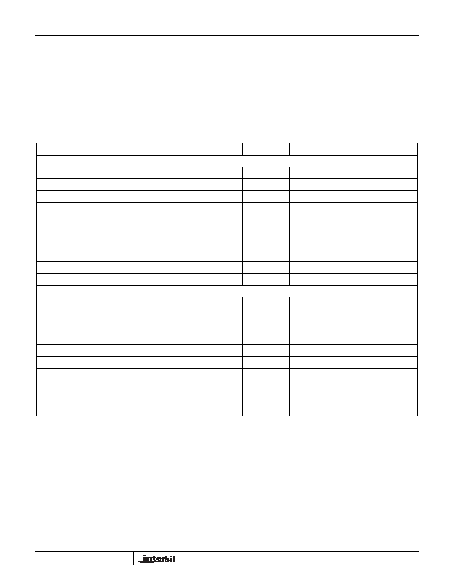
Open-Loop DC Electrical Specifications
Supplies at ±15V, Load = 1k
PARAMETER
DESCRIPTION
TEMP
MIN
TYP
MAX
UNITS
AMPLIFIER SECTION (NOT RESTORED)
V
OS
Input Offset Voltage
+25∞C
2
15
mV
I
B
+
I
IN
+ Input Bias Current
+25∞C
0.2
5
µA
I
B
-
I
IN
- Input Bias Current
+25∞C
10
65
µA
R
OL
Transimpedance (Note 1)
+25∞C
100
220
k
R
IN
-
I
N
- Resistance
+25∞C
50
CMRR
Common-Mode Rejection Ratio (Note 2)
+25∞C
50
56
dB
PSRR
Power Supply Rejection Ratio (Note 3)
+25∞C
50
70
dB
V
O
Output Voltage Swing; R
L
= 1k
+25∞C
±12
±13
V
I
SC
Short-Circuit Current
+25∞C
45
70
100
mA
I
SY
Supply Current (Quiescent)
+25∞C
10
20
32
mA
RESTORING SECTION
V
OS
, COMP
Composite Input Offset Voltage (Note 4)
+25∞C
8
35
mV
I
B
+,
R
Restore I
N
+ Input Bias Current
+25∞C
0.2
5
µA
I
OUT
Restoring Current Available
+25∞C
2
4
mA
PSRR
Power Supply Rejection Ratio (Note 3)
+25∞C
50
70
dB
G
OUT
Conductance
+25∞C
8
mA/V
I
SY
, RES
Supply Current, Restoring
+25∞C
10
23
37
mA
V
IL
, RES
RES Logic Low Threshold
+25∞C
1.0
1.4
V
V
IH
, RES
RES Logic High Threshold
+25∞C
1.4
1.8
V
I
IL
, RES
RES Input Current, Logic Low
+25∞C
2
10
µA
I
IH
, RES
RES Input Current, Logic High
+25∞C
0.5
3
µA
EL4390

3
NOTES:
1. Test fixture was designed to minimize capacitance at the I
N
- input. A "good" fixture should have less than 2pF of stray capacitance to ground at
this very sensitive pin. See application notes for further details.
2. SR is measured at 20% to 80% of 4Vpk-pk square wave, with A
V
= 5, R
F
= 820
, R
G
= 200
.
3. DC offset from -0.714V to +0.714V, AC amplitude is 286mV
P-P
, equivalent to 40 ire.
These numbers represent the worst case bias current, and
the worst case charging current. Note that to get the full
(2mA+) charging current, the clamp input must have
>250mV of error voltage.
Note that the magnitude of the bias current will decrease as
temperature increases.
The basic droop formula is:
V (droop) = I
B+
◊
(Line time - Charge time) / capacitor value
and the basic charging formula is:
V (charge) = I
OUT
◊
Charge time / capacitor value
Where I
OUT
is:
I
OUT
= (Clamp voltage - IN+ voltage) / 120
Closed-Loop AC Electrical Specifications
Supplies at ±15V, Load = 150
and 15pF, T
A
= 25∞C (Note 1)
PARAMETER
DESCRIPTION
MIN
TYP
MAX
UNITS
AMPLIFIER SECTION
SR
Slew Rate (Note 1)
800
V/µs
SR
Slew Rate w/ ±5V Supplies (Note 2)
550
V/µs
BW
Bandwidth, -3dB, A
V
= 1
±5V Supplies, -3dB
95
72
MHz
MHz
BW
Bandwidth, -0.1dB
±5V Supplies, -0.1dB
20
14
MHz
MHz
dG
Differential Gain at 3.58MHz
at ±5V Supplies (Note 3)
0.02
0.02
%
%
d
Differential Phase at 3.58MHz
at ±5V Supplies (Note 3)
0.03
0.06
(∞)
(∞)
RESTORING SECTION
T
RE
Time to Enable Restore
35
ns
T
RD
Time to Disable Restore
35
ns
TABLE 1. CHARGE STORAGE CAPACITOR VALUE VS.
DROOP AND CHARGING RATES
CAP VALUE
(NF)
DROOP IN
60µS (MV)
CHARGE IN
2µS (MV)
CHARGE IN
4µS (MV)
10
30
400
800
22
13.6
182
364
47
6.4
85
170
100
3.0
40
80
220
1.36
18
36
EL4390

4
Typical Performance Curves
Gain Flatness for Various R
F
V
S
= ±15V, A
V
= 0dB
Gain Flatness for Various R
F
V
S
= ±5V, A
V
= 0dB
Gain Flatness
for Various R
F
and R
G
Values
V
S
= ±15V, A
V
= 6dB
Phase Shift for A
V
= 2,
R
F
= R
G
= 1000
at V
S
= ±5V and V
S
= ±15V
Phase Shift for A
V
= 2,
R
F
= R
G
= 1300
Gain Flatness
for Various R
F
and R
G
Values
V
S
= ±5V, A
V
= 6dB
Gain Flatness
V
S
= ±15V, A
V
= 14dB,
R
F
/R
G
as Shown
Gain Flatness
V
S
= ±5V, A
V
= 14dB,
R
F
/R
G
as Shown
Phase Shift
for A
V
= 5dB, R
F
= 820
,
R
G
= 200
, V
S
= ±5V
EL4390

5
Typical Performance Curves
(Continued)
Gain Flatness
V
S
= ±5V, A
V
= 20dB,
R
F
/R
G
as Shown
Gain Flatness
V
S
= ±5V, A
V
= 26dB,
R
F
= 680
, R
G
= 36
Differential Gain
at V
S
= ±15V
Differential Phase
at V
S
= ±5V
Differential Gain
at V
S
= ±5V
Differential Phase
at V
S
= ±15V
Frequency Response
for Various C
LOAD
, V
S
= ±15V,
R
F
= R
G
= 1300
Frequency Response
for Various C
LOAD
, V
S
= ±5V,
R
F
= R
G
= 1300
Crosstalk,
Channel R and B to Channel G,
V
S
= ±5V, R
F
= 1300
EL4390