 | –≠–ª–µ–∫—Ç—Ä–æ–Ω–Ω—ã–π –∫–æ–º–ø–æ–Ω–µ–Ω—Ç: EL4431CN | –°–∫–∞—á–∞—Ç—å:  PDF PDF  ZIP ZIP |
1
Æ
FN7167
CAUTION: These devices are sensitive to electrostatic discharge; follow proper IC Handling Procedures.
1-888-INTERSIL or 321-724-7143
|
Intersil (and design) is a registered trademark of Intersil Americas Inc.
Copyright © Intersil Americas Inc. 2003. All Rights Reserved. Elantec is a registered trademark of Elantec Semiconductor, Inc.
All other trademarks mentioned are the property of their respective owners.
EL4430, EL4431
Video Instrumentation Amplifiers
The EL4430 and EL4431 are video
instrumentation amplifiers which are
ideal for line receivers, differential-to-
single-ended converters, transducer interfacing, and any
situation where a differential signal must be extracted from a
background of common-mode noise or DC offset.
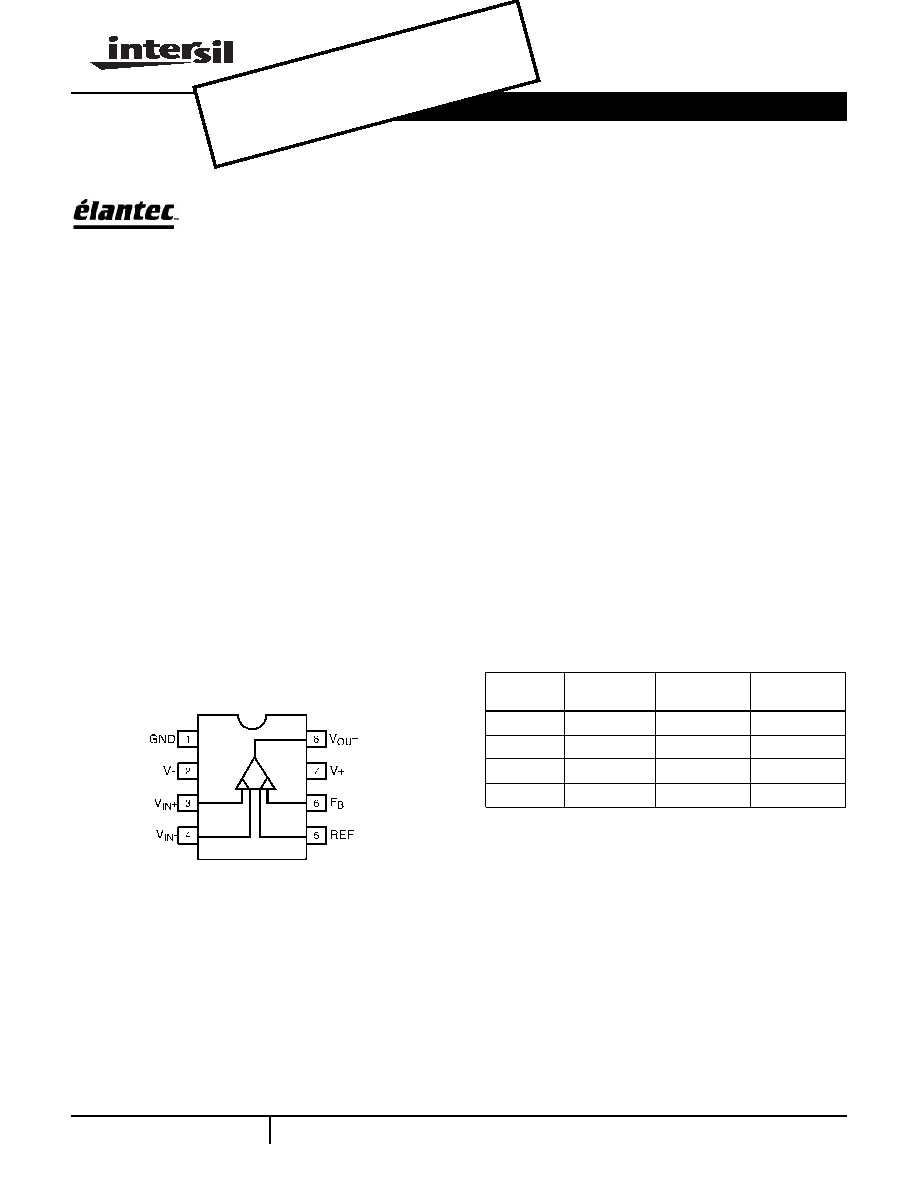
These devices have two differential signal inputs and two
differential feedback terminals. The FB terminal connects to
the amplifier output, or a divided version of it to increase
circuit gain, and the REF terminal is connected to the output
ground or offset reference.
The EL4430 is compensated to be stable at a gain of 1 or
more, and the EL4431 for a gain of 2 or more.
The amplifiers have an operational temperature of -40∞C to
+85∞C and are packaged in plastic 8-pin DIP and SO-8.
The EL4430 and EL4431 are fabricated with Elantec's
proprietary complementary bipolar process which gives
excellent signal symmetry and is free from latchup.
Pinout
Features
∑ Fully differential inputs and feedback
∑ Differential input range of ±2V
∑ Common-mode range of ±12V
∑ High CMRR at 4MHz of 70dB
∑ Stable at gains of 1, 2
∑ Calibrated and clean input clipping
∑ EL4430--80MHz @ G = 1
∑ EL4431--160MHz GBWP
∑ 380V/µs slew rate
∑ 0.02% or ∞ differential gain or phase
∑ Operates on ±5 to ±15V supplies with no AC degradation
Applications
∑ Line receivers
∑ "Loop-through" interface
∑ Level translation
∑ Magnetic head pre-amplification
∑ Differential-to-single-ended conversion
EL4430, EL4431
(8-PIN PDIP, SO)
TOP VIEW
Ordering Information
PART
NUMBER
TEMP. RANGE
PACKAGE
PKG. NO.
EL4430CN
-40∞C to +85∞C
8-Pin PDIP
MDP0031
EL4430CS
-40∞C to +85∞C
8-Pin SO
MDP0027
EL4431CN
-40∞C to +85∞C
8-Pin PDIP
MDP0031
EL4431CS
-40∞C to +85∞C
8-Pin SO
MDP0027
Data Sheet
January 1996, Rev. D
OBS
OLE
TE P
ROD
UCT
NO R
ECO
MME
NDE
D RE
PLA
CEM
ENT
cont
act o
ur T
echn
ical
Sup
port
Cen
ter a
t
1-88
8-IN
TER
SIL
or w
ww.
inte
rsil.c
om/t
sc

2
Absolute Maximum Ratings
(T
A
= 25∞C)
V+
Positive Supply Voltage . . . . . . . . . . . . . . . . . . . . . . . . . 16.5V
V
S
V+ to V- Supply Voltage . . . . . . . . . . . . . . . . . . . . . . . . . .33V
V
IN
Voltage at any Input or Feedback . . . . . . . . . . . . . . . V+ to V-
V
IN
Difference between Pairs of Inputs or Feedback. . . . . . . . .6V
I
IN
Current into any Input, or Feedback Pin . . . . . . . . . . . . . 4mA
I
OUT
Continuous Output Current . . . . . . . . . . . . . . . . . . . . . . 30mA
P
D
Maximum Power Dissipation . . . . . . . . . . . . . . . . See Curves
T
A
Operating Temperature Range . . . . . . . . . . . . -40∞C to +85∞C
T
S
Storage Temperature Range. . . . . . . . . . . . . -60∞C to +150∞C
CAUTION: Stresses above those listed in "Absolute Maximum Ratings" may cause permanent damage to the device. This is a stress only rating and operation of the
device at these or any other conditions above those indicated in the operational sections of this specification is not implied.
IMPORTANT NOTE: All parameters having Min/Max specifications are guaranteed. Typical values are for information purposes only. Unless otherwise noted, all tests
are at the specified temperature and are pulsed tests, therefore: T
J
= T
C
= T
A
Open-Loop DC Electrical Specifications
Power supplies at ±5V, T
A
= 25∞C. For the EL4431, R
F
= R
G
= 500
.
PARAMETER
DESCRIPTION
MIN
TYP
MAX
UNITS
V
DIFF
Differential input voltage (V
CM
= 0)
Clipping
2.0
2.3
V
0.1% nonlinearity
1.8
V
V
CM
Common-mode range (V
DIFF
= 0)
V
S
= ±5V
±2
±3.0
V
V
S
= ±15V
±12
±13.0
V
V
OS
Input offset voltage
2
8
mV
I
B
Input bias current (IN+, IN-, REF, and FB terminals)
12
20
µA
I
OS
Input offset current between IN+ and IN- and between REF and FB
0.2
2
µA
R
IN
Input resistance
100
230
k
CMRR
Common-mode rejection ratio
70
90
dB
PSRR
Power supply rejection ratio
60
dB
E
G
Gain error, excluding feedback resistors
-1.5
-0.2
+0.5
%
V
O
Output voltage swing EL4430
V
S
= ±5V
±2
±2.8
V
V
S
= ±15V
±12
±12.8
V
Output voltage swing EL4431
V
S
= ±5V
±2.5
±3.0
V
V
S
= ±15V
±12.5
±13.0
V
I
SC
Output short-circuit current
40
90
mA
I
S
Supply current, V
S
= ±15V
13.5
16
mA
EL4430, EL4431
3
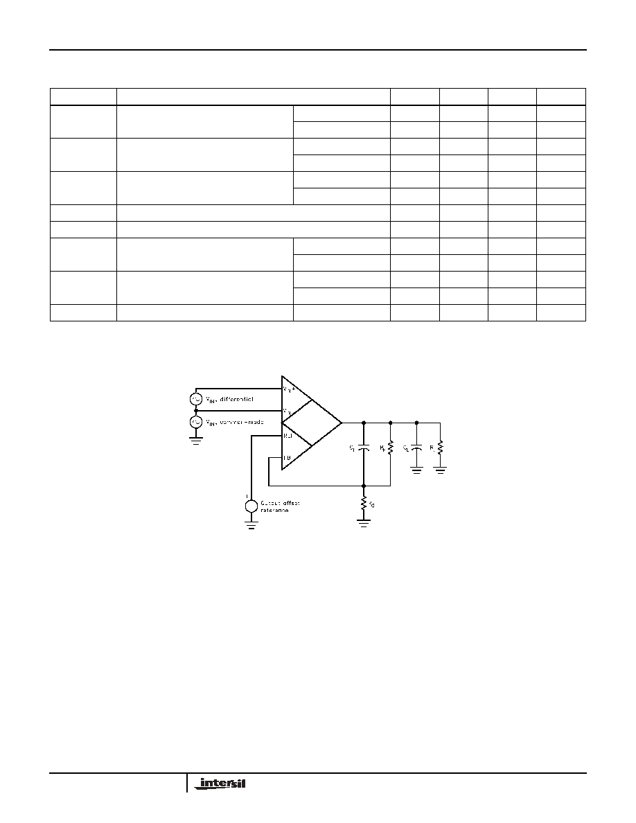
Test Circuit
Closed-Loop AC Electrical Specifications
Power supplies at ±12V, T
A
= 25∞C, R
L
= 500
for the EL4430, R
L
= 150
for the
EL4431, C
L
= 15pF. For the
EL4431, R
F
= R
G
= 500
.
PARAMETER
DESCRIPTION
MIN
TYP
MAX
UNITS
BW, -3dB
-3dB small-signal bandwidth
EL4430
82
MHz
EL4431
80
MHz
BW, ±0.1dB
0.1dB flatness bandwidth
EL4430
20
MHz
EL4431
14
MHz
Peaking
Frequency response peaking
EL4430
0.6
dB
EL4431
1.0
dB
SR
Slew rate, V
OUT
between -2V and +2V
380
V/µs
V
N
Input-referred noise voltage density
26
nV/
Hz
dG
Differential gain error, Voffset between
-0.7V and +0.7V
EL4430
0.02
%
EL4431, R
L
= 150
0.04
%
d
Differential gain error, Voffset between
-0.7V and +0.7V
EL4430
0.02
(∞)
EL4431, R
L
= 150
0.08
(∞)
T
S
Settling time, to 0.1% from a 4V step
EL4430
48
ns
EL4430, EL4431

4
Typical Performance Curves
EL4430 and EL4431
Common-Mode Rejection
Ratio vs Frequency
EL4430 Frequency Response
vs Gain
EL4430 Frequency Response
for Various R
L
, C
L
V
S
= ±5V
EL4430 Frequency Response
for Various R
L
, C
L
V
S
= ±15V
EL4431 Frequency Response
vs Gain
EL4431 Frequency Response
for Various R
L
, C
L
V
S
= ±5V
EL4431 Frequency Response
for Various R
L
, C
L
V
S
= ±15V
EL4430 Differential Gain
and Phase vs Input Offset
Voltage for V
S
= ±5V
EL4430 Differential Gain
and Phase vs Input Offset
Voltage for V
S
= ±12V
EL4430 Differential Gain
and Phase Error vs R
L
EL4430, EL4431

5
Typical Performance Curves
(Continued)
EL4431 Differential Gain
and Phase vs Input Offset
Voltage for V
S
= ±5V
EL4431 Differential Gain
and Phase vs Input Offset
Voltage for V
S
= ±12V
EL4431 Differential Gain
and Phase Error vs R
L
EL4430 Nonlinearity
vs Input Signal Span
EL4431 Nonlinearity
vs Input Signal Span
EL4430 -3dB Bandwidth
and Peaking vs Supply
Voltage for A
V
= +1
EL4430 -3dB Bandwidth
and Peaking vs Die
Temperature for A
V
= +1
EL4430 Gain, -3dB Bandwidth
and Peaking vs Load Resistance
for A
V
= +1
EL4431 -3dB Bandwidth
and Peaking
vs Supply Voltage
EL4431 -3dB Bandwidth
and Peaking vs Die
Temperature for A
V
= +2
EL4431 Gain, -3dB Bandwidth
and Peaking vs Load
Resistance for A
V
= +2
EL4430, EL4431