 | –≠–ª–µ–∫—Ç—Ä–æ–Ω–Ω—ã–π –∫–æ–º–ø–æ–Ω–µ–Ω—Ç: EL4442 | –°–∫–∞—á–∞—Ç—å:  PDF PDF  ZIP ZIP |

1
Æ
FN7166
CAUTION: These devices are sensitive to electrostatic discharge; follow proper IC Handling Procedures.
1-888-INTERSIL or 321-724-7143
|
Intersil (and design) is a registered trademark of Intersil Americas Inc.
Copyright © Intersil Americas Inc. 2003. All Rights Reserved. Elantec is a registered trademark of Elantec Semiconductor, Inc.
All other trademarks mentioned are the property of their respective owners.
EL4421, EL4422, EL4441,
EL4442, EL4443, EL4444
Multiplexed-Input Video Amplifiers
The EL44XX family of video
multiplexed-amplifiers offers a very
quick 8ns switching time and low glitch
along with very low video distortion. The amplifiers have
good gain accuracy even when driving low-impedance loads.
To save power, the amplifiers do not require heavy loading to
remain stable.
The EL4421 and EL4422 are two-input multiplexed
amplifiers. The -inputs of the input stages are wired together
and the device can be used as a pin-compatible upgrade
from the MAX453.
The EL4441 and EL4442 have four inputs, also with
common feedback. These may be used as upgrades of the
MAX454.
The EL4443 and EL4444 are also 4-input multiplexed
amplifiers, but both positive and negative inputs are wired
separately. A wide variety of gain- and phase-switching
circuits can be built using independent feedback paths for
each channel.
The EL4421, EL4441, and EL4443 are internally
compensated for unity-gain operation. The EL4422, EL4442,
and EL4444 are compensated for gains of +2 or more,
especially useful for driving back-matched cables.
The amplifiers have an operational temperature of -40∞C to
+85∞C and are packaged in plastic 8- and 14-pin DIP and 8-
and 14-pin SO.
The EL44XX multiplexed-amplifier family is fabricated with
Elantec's proprietary complementary bipolar process which
gives excellent signal symmetry and is very rugged.
Pinouts
Features
∑ Unity or + 2-gain bandwidth of 80MHz
∑ 70dB off-channel isolation at 4MHz
∑ Directly drives high-impedance or 75
loads
∑ 0.02% and 0.02∞ differential gain and phase errors
∑ 8ns switching time
∑ < 100mV switching glitch
∑ 0.2% loaded gain error
∑ Compatible with ±3V to ±15V supplies
∑ 160mW maximum dissipation at ±5V supplies
EL4421/EL4422
(8-PIN PDIP, SO)
TOP VIEW
EL4441/EL4442
(14-PIN PDIP, SO)
TOP VIEW
EL4443/EL4444
(14-PIN PDIP, SO)
TOP VIEW
Manufactured under U.S. Patent No. 5,352,987
Ordering Information
PART
NIMBER
TEMP. RANGE
PACKAGE
PKG. NO.
EL4421CN
-40∞C to +85∞C
8-Pin PDIP
MDP0031
EL4421CS
-40∞C to +85∞C
8-Pin SO
MDP0027
EL4422CN
-40∞C to +85∞C
8-Pin PDIP
MDP0031
EL4422CS
-40∞C to +85∞C
8-Pin SO
MDP0027
EL4441CN
-40∞C to +85∞C
14-Pin PDIP
MDP0031
EL4441CS
-40∞C to +85∞C
14-Pin SO
MDP0027
EL4442CN
-40∞C to +85∞C
14-Pin PDIP
MDP0031
EL4442CS
-40∞C to +85∞C
14-Pin SO
MDP0027
EL4443CN
-40∞C to +85∞C
14-Pin PDIP
MDP0031
EL4443CS
-40∞C to +85∞C
14-Pin SO
MDP0027
EL4444CN
-40∞C to +85∞C
14-Pin PDIP
MDP0031
EL4444CS
-40∞C to +85∞C
14-Pin SO
MDP0027
Data Sheet
January 1996, Rev. C
OBS
OLET
E PR
ODU
CT
NO R
ECO
MME
NDED
REP
LACE
MEN
T
conta
ct ou
r Tec
hnica
l Sup
port
Cent
er at
1-888
-INTE
RSIL
or w
ww.in
tersil
.com
/tsc

2
NOTES:
1. The '21, '41, and '43 devices are connected for unity-gain operation with 75
load and an input span of ±1V. The '22, '42, and '44 devices are
connected for a gain of +2 with a 150
load and a ±1V input span with R
F
= R
G
= 270
.
2. The '21 and '41 devices are connected for unity gain with a ±3V input span while the output swing is measured.
3. CMIR is assured by passing the CMRR test at input voltage extremes.
Absolute Maximum Ratings
(T
A
= 25∞C)
V+
Positive Supply Voltage . . . . . . . . . . . . . . . . . . . . . . 16.5V
V
S
V+ to V- Supply Voltage . . . . . . . . . . . . . . . . . . . . . . . .33V
V
IN
Voltage at any Input or Feedback . . . . . . . . . . . . V+ to V-
V
IN
Difference between Pairs of Inputs or Feedback . . . . . .6V
V
LOGIC
Voltage at A0 or A1 . . . . . . . . . . . . . . . . . . . . . . -4V to 6V
I
IN
Current into any Input, Feedback, or Logic Pin . . . . . 4mA
I
OUT
Output Current. . . . . . . . . . . . . . . . . . . . . . . . . . . . . 30mA
P
D
Maximum Power Dissipation . . . . . . . . . . . . . See Curves
CAUTION: Stresses above those listed in "Absolute Maximum Ratings" may cause permanent damage to the device. This is a stress only rating and operation of the
device at these or any other conditions above those indicated in the operational sections of this specification is not implied.
IMPORTANT NOTE: All parameters having Min/Max specifications are guaranteed. Typical values are for information purposes only. Unless otherwise noted, all tests
are at the specified temperature and are pulsed tests, therefore: T
J
= T
C
= T
A
Open-Loop DC Electrical Specifications
Power supplies at ±5V, T
A
= 25∞C, R
L
= 500
, unless otherwise specified
PARAMETER
DESCRIPTION
MIN
TYP
MAX
UNITS
V
OS
Input Offset Voltage
'21, '41, and '43
-9
±3
9
mV
'22, '42, and '44
-7
±2
7
I
B
Input Bias Current, Positive Inputs Only of the '21, '22, '41, '42, and All Inputs of
the '43 and '44
-12
-5
0
µA
I
FB
Input Bias Currents of Common
Feedback
'21 and '22
-24
-10
0
µA
'41 and '42
-48
-20
0
µA
I
OS
Input Offset Currents of the '43 and '44
60
350
nA
E
G
Gain Error (Note 1)
'21 and '41 and '43
0.2
0.6
%
'22, '42 and '44
0.1
0.6
V/V
A
VOL
Open-Loop Gain (Note 1)
EL4443
350
500
V/V
EL4444
500
750
V/V
V
IN
Input Signal Range, EL4421 and EL4441 (Note 2)
±2.5
±3
V
CMRR
Common-Mode Rejection Ratio, EL4443 and EL4444
70
90
dB
PSRR
Power Supply Rejection Ratio V
S
from ±5V to ±15V
60
70
dB
CMIR
Common-Mode Input Range EL4443 and EL4444 (Note 3)
±2.5
±3
V
V
OUT
Output Swing
±2.5
±3.5
V
I
SC
Output Short-Circuit Current
±40
±80
mA
F
T
Unselected Channel Feedthrough
Attenuation (Note 1)
'21, '41, '43
70
80
dB
'22, '42, '44
55
64
dB
I
LOGIC
Input Current at A0 and A1 with Input = 0V and 5V
-16
-8
0
µA
V
LOGIC
Logic Valid High and Low Input Levels
0.8
2.0
V
I
S
Supply Current
EL4421 and EL4422
11
14
mA
EL4441, EL4442, EL4443, and EL4444
13
16
EL4421, EL4422, EL4441, EL4442, EL4443, EL4444

3
Closed-Loop AC Electrical Specifications
Power supplies at ±5V. T
A
= 25∞C, for EL4421, EL4441, and EL4443 A
V
= +1 and
R
L
= 500
, for EL4422, EL4442, and EL4444 A
V
= +2 and R
L
= 150
with
R
F
= R
G
= 270
and C
F
= 3pF; for all C
L
= 15pF
PARAMETER
DESCRIPTION
MIN
TYP
MAX
UNITS
BW - 3dB
-3dB Small-Signal Bandwidth
EL4421, '41, '43
80
MHz
EL4422, '42, '44
65
MHz
BW ± 0.1dB
0.1dB Flatness Bandwidth
10
MHz
Peaking
Frequency Response Peaking
0.5
dB
SR
Slewrate, V
OUT
between -2.5V
and +2.5V, V
S
= ±12V
EL4421, EL4441, EL4443
150
200
V/µsec
EL4422, EL4442, EL4444
180
240
V/µsec
V
N
Input-Referred Noise Voltage
Density
EL4421, EL4441, EL4443
18
nV/
Hz
EL4422, EL4442, EL4444
14
nV/
Hz
d
G
Differential Gain Error, V
OFFSET
between -0.7V and +0.7V
EL4421, '41, '43 (V
S
= ±12V)
0.01
%
EL4421, '41, '43 (V
S
= ±5V)
0.10
%
EL4422, '42, '44 (V
S
= ±12V)
0.02
%
EL4422, '42, '44 (V
S
= ±5V)
0.11
%
d
ÿ
Differential Phase Error, V
OFFSET
between -0.7V and +0.7V
EL4421, '41, '43 (V
S
= ±12V)
0.01
∞
EL4421, '41, '43 (V
S
= ±5V)
0.1
∞
EL4422, '42, '44 (V
S
= ±12V)
0.02
∞
EL4422, '42, '44 (V
S
= ±5V)
0.15
∞
T
MUX
Multiplex Delay Time, Logic
Threshold to 50% Signal Change
EL4421, '22
8
nsec
EL4441, '42, '43, '44
12
nsec
V
GLITCH
Peak Multiplex Glitch
EL4421, '22
70
mV
EL4441, '42, '43, '44
100
mV
ISO
Channel Off Isolation at 3.58MHz
(See Text)
EL4421, EL4441, EL4443
76
dB
EL4422, EL4442, EL4444
63
dB
EL4421, EL4422, EL4441, EL4442, EL4443, EL4444
4
Typical Performance Curves
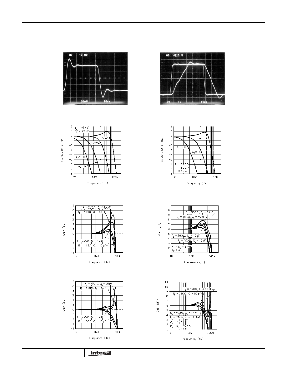
EL4421, EL4441, and EL4443
Frequency Response for
Various Gains
EL4421, EL4441, and EL4443
Large-Signal Response
V
S
= ±12V, R
L
= 500
EL4422, EL4442, and EL4444
Frequency Response for
Various Gains
EL4421, EL4441, and EL4443
Small-Signal Transient Response
V
S
= ±5V, R
L
= 500
EL4421, EL4441, and EL4443
Frequency Response for Various Loads
V
S
= ±5V, A
V
= +1
EL4422, EL4442, and EL4444
Frequency Response for Various Loads
V
S
= ±5V, A
V
= +2
Frequency Response
for Various Loads
V
S
= ±15V, A
V
= + 1
EL4422, EL4442, and EL4444
Frequency Response for Various Loads
V
S
= ±15V, A
V
= +2
EL4421, EL4422, EL4441, EL4442, EL4443, EL4444

5
Typical Performance Curves
(Continued)
EL4443 Open-Loop Gain and
Phase vs. Frequency
EL4444 Open-Loop Gain and
Phase vs. Frequency
EL4421, EL4441, and EL4443
-3dB Bandwidth, Slewrate, and
Peaking vs. Supply Voltage
EL4422, EL4442, and EL4444
-3dB Bandwidth, Slewrate, and
Peaking vs. Supply Voltage
EL4421, EL4441, and EL4443
Bandwidth, Slewrate, and Peaking vs. Temperature,
A
V
= +1, R
L
=500
EL4422, EL4442, and EL4444
Bandwidth, Slewrate, and Peaking vs. Temperature,
A
V
= +2, R
L
= 150
, R
I
= R
G
= 270
, C
F
= 3pF
EL4421, EL4441, and EL4443
-3dB Bandwidth and Gain Error vs. Load
Resistance
Input Noise vs. Frequency
EL4421, EL4422, EL4441, EL4442, EL4443, EL4444