
1
Æ
FN7009.7
EL4511
Super Sync Separator
The EL4511 sync separator IC is designed for operation in
the next generation of DTV, HDTV, and projector
applications, as well as broadcast equipment and other
applications where video signals need to be processed.
The EL4511 accepts sync on green, separate sync, and H/V
sync inputs, automatically selecting the relevant format. It is
also capable of detecting and decoding tri-level syncs used
with the latest HD systems. Unlike standard sync separators,
the EL4511 can automatically detect the line rate and locks
to it, without the use of an external R
SET
resistor.
The EL4511 is available in a 24-pin QSOP package and
operates over the full 0∞C to 70∞C temperature range.
Features
∑ Composite, component, HDTV, and PC signal-compatible
∑ Tri-level & bi-level sync-compatible
∑ Auto sync detection
∑ 150kHz max line rate
∑ Low power
∑ Small package outline
∑ 3.3V and 5V operation
∑ Pb-Free Plus Anneal Available (RoHS Compliant)
Applications
∑ HDTV/DTV analog inputs
∑ Video projectors
∑ Computer monitors
∑ Set top boxes
∑ Security video
∑ Broadcast video equipment
Pinout
EL4511
(24-PIN QSOP)
TOP VIEW
Ordering Information
PART
NUMBER
PACKAGE
TAPE &
REEL
PKG. DWG. #
EL4511CU
24-Pin QSOP
-
MDP0040
EL4511CU-T7
24-Pin QSOP
7"
MDP0040
EL4511CU-T13
24-Pin QSOP
13"
MDP0040
EL4511CUZ
(See Note)
24-Pin QSOP
(Pb-Free)
-
MDP0040
EL4511CUZ-T7
(See Note)
24-Pin QSOP
(Pb-Free)
7"
MDP0040
EL4511CUZ-T13
(See Note)
24-Pin QSOP
(Pb-Free)
13"
MDP0040
NOTE: Intersil Pb-free plus anneal products employ special Pb-free
material sets; molding compounds/die attach materials and 100%
matte tin plate termination finish, which are RoHS compliant and
compatible with both SnPb and Pb-free soldering operations. Intersil
Pb-free products are MSL classified at Pb-free peak reflow
temperatures that meet or exceed the Pb-free requirements of
IPC/JEDEC J STD-020.
1
2
3
4
16
15
14
13
5
6
7
12
11
9
8
10
20
19
18
17
24
23
22
21
XTAL
VBLANK
SYNCLOCK
PDWN
SDENB
SCL
SDA
GNDD1
HIN
SYNCIN
VERTIN
LEVEL
XTALN
ODD/EVEN
VERTOUT
BACKPORCH
SYNCOUT
VCCD
GNDD2
GNDA2
VCCA2
VCCA1
GNDA1
HOUT
Data Sheet
July 21, 2005
CAUTION: These devices are sensitive to electrostatic discharge; follow proper IC Handling Procedures.
1-888-INTERSIL or 1-888-468-3774
|
Intersil (and design) is a registered trademark of Intersil Americas Inc.
Copyright © Intersil Americas Inc. 2002-2005. All Rights Reserved. All other trademarks mentioned are the property of their respective owners.
Manufactured under U.S. Patent 5,528,303
Manufactured under License, U.S. Patents 5,486,869; 5,754,250

2
FN7009.7
July 21, 2005
IMPORTANT NOTE: All parameters having Min/Max specifications are guaranteed. Typ values are for information purposes only. Unless otherwise noted, all tests are
at the specified temperature and are pulsed tests, therefore: T
J
= T
C
= T
A
Absolute Maximum Ratings
(T
A
= 25∞C)
Supply Voltage . . . . . . . . . . . . . . . . . . . . . . . . . . . (V
S
to GND) +6V
Pin Voltage. . . . . . . . . . . . . . . . . . . . . . . . . . . GND - 0.3V, V
S
+0.3V
V
CCA1
, V
CCA2
& V
CCD
. . . . . . . . . . . . . . . .Must Be Same Voltage
Power Dissipation . . . . . . . . . . . . . . . . . . . . . . . . . . . . . See Curves
Storage Temperature Range . . . . . . . . . . . . . . . . . .-65∞C to +150∞C
Operating Junction Temperature . . . . . . . . . . . . . . . . . . . . . . . 125∞C
Ambient Operating Temperature . . . . . . . . . . . . . . . . . 0∞C to +70∞C
CAUTION: Stresses above those listed in "Absolute Maximum Ratings" may cause permanent damage to the device. This is a stress only rating and operation of the
device at these or any other conditions above those indicated in the operational sections of this specification is not implied.
Electrical Specifications
V
S
= V
CCA1
= V
CCA2
= V
CCD
= +5V, T
A
= 25∞C, NTSC input signal on SYNCIN, no output loads, unless
otherwise specified.
PARAMETER
DESCRIPTION
CONDITIONS
MIN
TYP
MAX
UNIT
GENERAL
ISD
Digital Supply Current
(Note 1)
15
20
mA
Standby PDWN = V
CCD
(Note 2)
4
20
µA
ISA2
Rate Acquisition Oscillator Supply
Current
(Note 1)
3
20
mA
Standby PDWN = V
CCD
2.5
20
µA
ISA1
Analog Processing Supply Current
(Note 1)
3
20
mA
Standby PDWN = V
CCD
(Note 2)
3
20
µA
COMPOSITE SYNC INPUT AT SYNCIN
V
SYNC
Sync Signal Amplitude
AC coupled to SYNCIN pin (Notes 1 & 3)
140
600
mV
V
SLICE
Slicing Level of Sync Signal
After sync lock is attained, see description
50
%
HORIZONTAL AND VERTICAL INPUT AT H
IN
, VERTIN
H
SLICE
, V
SLICE
Slice Level of H
IN
and VERTIN
1.4
V
T
HINL
H Sync Width
(Bi-Level)
3
12.8
% of H
time
(Tri-Level)
Minimum Sync Width
1.4
% of H
time
F
HINH
H Sync Frequency
10.75
150
kHz
T
VINL
V Sync Width
2
7
H lines
F
VINH
V Sync Frequency
23
100
Hz
LOGIC OUTPUT SIGNALS, H
OUT
, V
OUT
, V
BLANK
, BACKPORCH, ODD/EVEN, SYNCLOCK
O/P
LOW
Logic Low State
1.6mA, V
CCD
= 5V
GNDD+0.4
V
1.6mA, V
CCD
= 3.3V
GNDD+0.5
O/P
HI
Logic High State
1.6mA, V
CCD
= 5V
V
CCD
-0.4
V
1.6mA, V
CCD
= 3.3V
V
CCD
-0.5
Td
HOUT
H
OUT
Timing Relative to Input
See timing diagrams 1, 2, 3 & 4
Td
SYNCOUT
SYNCOUT Timing Relative to Input See timing diagrams 1, 2, 3 & 4
Td
BACKPORCH
BACKPORCH Timing Relative to
Input
See timing diagrams 1, 2, 3 & 4
LEVEL OUTPUT DRIVER, LEVEL
V
LEVEL
2 X Amplitude of V
SYNC
Refer to description of operation
1.9x
2.15x
2.4x
Z
LEVEL
O/P Resistance of Driver Stage
450
EL4511
3
FN7009.7
July 21, 2005
REFERENCE OSCILLATOR
F
IN
Reference Input Frequency
Refer to description of operation
50
kHz
F
XTAL
Crystal Frequency
Watch crystal (optional)
32.768
kHz
CONTROL INTERFACE SIGNALS PDWN, SDENB, SCL AND SDA
V
HIGH
Input Logic High Threshold
V
CCD
-1V
V
LOW
Input Logic Low Threshold
V
GNDD
+1V
O/PV
HI
SDA O/P Logic High State
@ 1mA
V
CCD
-0.4
V
O/PV
LOW
SDA O/P Logic Low State
@ 1mA
GNDD+0.4
V
F
SCL
Serial Control Clock Frequency
5
MHz
T
CLS
Setup
Time
30
ns
T
CLH
Hold
Time
30
ns
T
LC
Load to Clock Time
30
ns
T
DC
Hold to Clock Time
30
ns
T
CD
Clock to Data Out Time
30
ns
NOTES:
1. NTSC signal; see curves for other rates.
2. XTAL pin must be low, otherwise 70µA.
3. I/P range reduces if V
S
of 3.3V - 4.5V (see Timing Diagram 1).
Electrical Specifications
V
S
= V
CCA1
= V
CCA2
= V
CCD
= +5V, T
A
= 25∞C, NTSC input signal on SYNCIN, no output loads, unless
otherwise specified.
(Continued)
PARAMETER
DESCRIPTION
CONDITIONS
MIN
TYP
MAX
UNIT
EL4511

4
FN7009.7
July 21, 2005
Pin Descriptions
PIN NUMBER
PIN NAME
PIN TYPE
PIN DESCRIPTION
1
XTAL
Input
Crystal input (see Table 2 for details)
2
VBLANK
Logic Output
Vertical blank output
3
SYNCLOCK
Logic Output
Indicates that the EL4511 has locked to the line rate and has found three consecutive
"good H lines"
4
PWDN
Logic Input
Power-down = hi
5
SDENB
Logic Input
Serial interface enable = low
6
SCL
Logic Input
Serial clock
7
SDA
Logic BIDIR
Serial data (input for chip setup, output for diagnostic information)
8
GNDD1
Power
Digital ground 1
9
HIN
Input
Horizontal sync
10
SYNCIN
Input
Video input, which may incorporate sync signal; connect to Y or G
11
VERTIN
Input
Vertical sync input
12
LEVEL
Output
Indicates 2x amplitude of sync tip vs. back porch; referred to ground
13
GNDA1
Power
Analog ground 1
14
VCCA1
Power
Analog power supply 1
15
VCCA2
Power
Analog power supply 2
16
GNDA2
Power
Analog ground 2
17
GNDD2
Power
Digital ground 2
18
VCCD1
Power
Digital power supply 1
19
SYNCOUT
Logic Output
Composite sync output
20
BACKPORCH
Logic Output
Back porch output
21
HOUT
Logic Output
Horizontal sync output
22
VERTOUT
Logic Output
Vertical sync output
23
ODD/EVEN
Logic Output
Odd-Even field indicator output
24
XTALN
Output
Crystal output (see Table 2 for details)
Typical Performance Curves
FIGURE 1. PACKAGE POWER DISSIPATION vs AMBIENT
TEMPERATURE
FIGURE 2. PACKAGE POWER DISSIPATION vs AMBIENT
TEMPERATURE
1.136W
JA
=8
8∞C
/W
QS
OP
24
1.4
1.2
1
0.8
0.6
0.2
0
0
25
50
75
100
150
AMBIENT TEMPERATURE (∞C)
POWE
R DI
SSI
PATI
ON (
W
)
125
85
JEDEC JESD51-7 HIGH EFFECTIVE
THERMAL CONDUCTIVITY TEST BOARD
0.4
870mW
JA
=11
5∞C
/W
QS
OP
24
1.2
1
0.8
0.6
0.4
0
0
25
50
75
100
150
AMBIENT TEMPERATURE (∞C)
POWE
R DI
SSI
PATI
ON (
W
)
125
85
JEDEC JESD51-3 LOW EFFECTIVE
THERMAL CONDUCTIVITY TEST BOARD
0.2
EL4511
5
FN7009.7
July 21, 2005
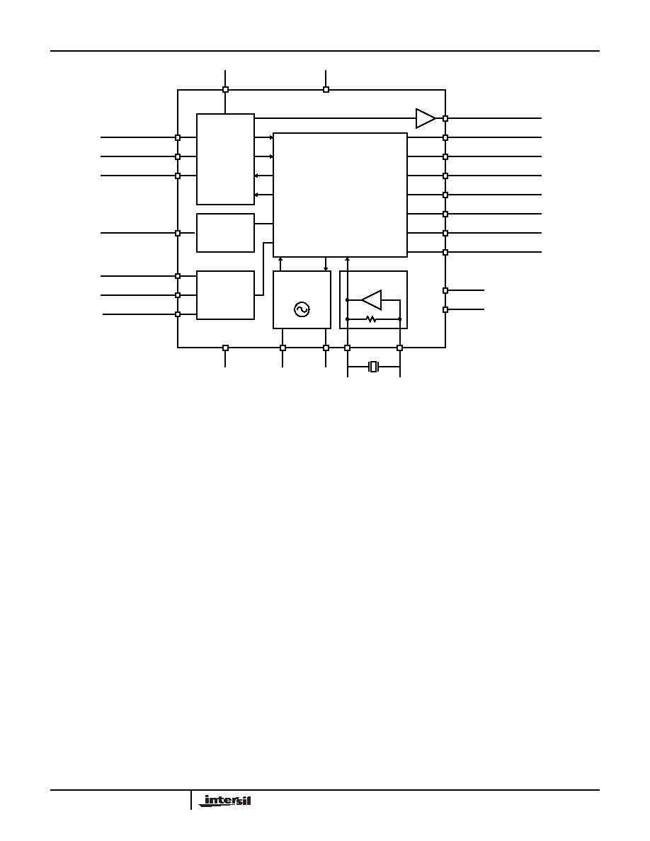
FIGURE 3. BLOCK DIAGRAM
LEVEL
HOUT
SYNCOUT
VERTOUT
VBLANK
BACKPORCH
ODD/EVEN
SYNCLOCK
SYNC LEVEL
HORIZONTAL O/P
COMP SYNC O/P
VERTICAL O/P
VERTICAL BLANKING O/P
BACK PORCH O/P
ODD/EVEN O/P
SYNC LOCK O/P
DIGITAL PROCESSING
RATE
ACQUISITION
OSCILLATOR
REFERENCE
OSCILLATOR
GNDD1
GNDD2
XTAL
XTALIN
GNDA2
VCCA2
SLICING
&
ANALOG
PROCESSING
RESET
SERIAL I/F
GNDA1
VERTIN
SYNCIN
HIN
SDENB
SCL
SDA
PDWN
VERTICAL SYNC
COMPOSITE SYNC
HORIZONTAL SYNC
LOW ACTIVE SERIAL
DATA ENABLE
SERIAL CLOCK
SERIAL DATA
POWER DOWN
VCCD
VCCA1
MODE CONTROL PINS
EL4511