 | –≠–ª–µ–∫—Ç—Ä–æ–Ω–Ω—ã–π –∫–æ–º–ø–æ–Ω–µ–Ω—Ç: EL4583 | –°–∫–∞—á–∞—Ç—å:  PDF PDF  ZIP ZIP |
1
Æ
FN7173.1
EL4583
Sync Separator, 50% Slice, S-H, Filter,
H
OUT
The EL4583 extracts timing from video sync in NTSC, PAL,
and SECAM systems, and non standard formats, or from
computer graphics operating at higher scan rates. Timing
adjustment is via an external resistor. Input without valid
vertical interval (no serration pulses) produces a default
vertical output.
Outputs are: composite sync, vertical sync, filter, burst/back
porch, horizontal, no signal detect, level, and odd/even
output (in interlaced scan formats only).
The EL4583 sync slice level is set to the mid-point between
sync tip and the blanking level. This 50% point is determined
by two internal sample and hold circuits that track sync tip
and back porch levels. It provides hum and noise rejection
and compensates for input levels of 0.5V to 2.0V
P-P
.
A built in filter attenuates the chroma signal to prevent color
burst from disturbing the 50% sync slice. Cut off frequency is
set by a resistor to ground from the Filter Cut Off pin.
Additionally, the filter can be by-passed and video signal fed
directly to the Video Input.
The level output pin provides a signal with twice the sync
amplitude which may be used to control an external AGC
function. A TTL/CMOS compatible No Signal Detect Output
flags a loss or reduction in input signal level. A resistor sets
the Set Detect Level.
The EL4583 is manufactured using Elantec's high
performance analog CMOS process.
Pinout
Features
∑ NTSC, PAL, and SECAM sync separation
∑ Single supply, +5V operation
∑ Precision 50% slicing
∑ Built-in programmable color burst filter
∑ Decodes non-standard vertical
∑ Horizontal sync output
∑ Sync. pulse amplitude output
∑ Same socket can be used for 8-pin EL4581
∑ Low-power CMOS
∑ Detects loss of signal
∑ Resistor programmable scan rate
∑ Few external components
∑ Available in 16-pin PDIP and 16-pin SO (0.150") packages
∑ Pb-Free Plus Anneal Available (RoHS Compliant)
Applications
∑ Video special effects
∑ Video test equipment
∑ Video distribution
∑ Multimedia
∑ Displays
∑ Imaging
∑ Video data capture
∑ Video triggers
1
2
3
4
16
15
14
13
5
6
7
12
11
10
8
9
FILTER CUT OFF
SET DETECT LEVEL
COMPOSITE SYNC OUT
FILTER INPUT
VERTICAL SYNC OUT
DIGITAL GND
FILTER OUTPUT
COMPOSITE VIDEO INPUT
ANALOG GND
HORIZONTAL SYNC OUT
VDD
ODD/EVEN OUTPUT
RSET*
BURST/BACK PORCH OUTPUT
NO SIGNAL DETECT OUTPUT
LEVEL OUTPUT
EL4583
(16-PIN SO, PDIP)
TOP VIEW
*Note: R
SET
must be a 1% register
Ordering Information
PART NUMBER
PACKAGE
TAPE &
REEL
PKG.
DWG. #
EL4583CN
16-Pin PDIP
-
MDP0031
EL4583CS
16-Pin SO (0.150")
-
MDP0027
EL4583CS-T7
16-Pin SO (0.150")
7"
MDP0027
EL4583CS-T13
16-Pin SO (0.150")
13"
MDP0027
EL4583CSZ (Note) 16-Pin SO (0.150") (Pb-free)
-
MDP0027
EL4583CSZ-T7
(Note)
16-Pin SO (0.150") (Pb-free)
7"
MDP0027
EL4583CSZ-T13
(Note)
16-Pin SO (0.150") (Pb-free)
13"
MDP0027
NOTE: Intersil Pb-free plus anneal products employ special Pb-free
material sets; molding compounds/die attach materials and 100%
matte tin plate termination finish, which are RoHS compliant and
compatible with both SnPb and Pb-free soldering operations. Intersil
Pb-free products are MSL classified at Pb-free peak reflow
temperatures that meet or exceed the Pb-free requirements of
IPC/JEDEC J STD-020.
Data Sheet
June 27, 2005
CAUTION: These devices are sensitive to electrostatic discharge; follow proper IC Handling Procedures.
1-888-INTERSIL or 1-888-468-3774
|
Intersil (and design) is a registered trademark of Intersil Americas Inc.
Copyright Intersil Americas Inc. 2002, 2003, 2005. All Rights Reserved
All other trademarks mentioned are the property of their respective owners.

2
NOTES:
1. No video signal, outputs unloaded
2. At loss of signal (pin 10 high) the pull down current source switches to a value of 10µA
3. Tested for V
DD
5V ±5%
4. Current sourced from pin 2 is V
REF
/R
SET
NOTES:
1. Width is a function of R
SET
2. c/s, Vertical, Back porch and H are all active low, V
OH
= 0.8V; vertical is 3H lines wide of NTSC signal
3. Attenuation is a function of R
F
. See filter typical characteristics
4. Vertical pulse width in absence of serrations on input signal
Absolute Maximum Ratings
(T
A
= 25∞C)
V
CC
Supply . . . . . . . . . . . . . . . . . . . . . . . . . . . . . . . . . . . . . . . . . .7V
Storage Temperature. . . . . . . . . . . . . . . . . . . . . . . .-65∞C to +150∞C
Pin Voltages. . . . . . . . . . . . . . . . . . . . . . . . . . . . -0.5V to V
CC
+0.5V
Operating Temperature Range . . . . . . . . . . . . . . . . .-40∞C to +85∞C
Power Dissipation . . . . . . . . . . . . . . . . . . . . . . . . . . . . . See Curves
Die Junction Temperature . . . . . . . . . . . . . . . . . . . . . . . . . . . . 150∞C
CAUTION: Stresses above those listed in "Absolute Maximum Ratings" may cause permanent damage to the device. This is a stress only rating and operation of the
device at these or any other conditions above those indicated in the operational sections of this specification is not implied.
IMPORTANT NOTE: All parameters having Min/Max specifications are guaranteed. Typical values are for information purposes only. Unless otherwise noted, all tests
are at the specified temperature and are pulsed tests, therefore: T
J
= T
C
= T
A
DC Electrical Specifications
V
DD
= 5V, T
A
= 25∞C, R
SET
= 681k
, R
F
= 22k
, R
LV
= 82k
PARAMETER
DESCRIPTION
MIN
TYP
MAX
UNIT
I
DD
V
DD
= 5V (Note 1)
2.5
4
mA
Clamp Voltage
Pins 4, 8, unloaded
1.3
1.55
1.8
V
Discharge Current
Pins 4, 8, with Signal (V
IN
= 2V)
3
6
12
µA
Discharge Current
Pins 4, 8, no Signal (Note 2)
10
µA
Clamp Charge Current
Pins 4, 8, V
IN
= 1V
2
3
4
mA
Ref. Voltage V
REF
Pin 12, V
DD
= 5V (Note 3)
1.5
1.75
2
V
Filter Reference Voltage, VRF
Pin 1
0.35
0.5
0.65
V
Level Reference Current
Pin 2 (Note 4)
1.5
2.5
3.5
µA
V
OL
Output Low Voltage
I
OL
= 1.6mA
350
800
mV
V
OH
Output High Voltage
I
OH
= -40µA
4
V
I
OH
= -1.6mA
2.4
4
V
Dynamic Specifications
R
F
= 22k
, R
SET
= 681k
, V
DD
= 5V, Video Input = 1V
P-P
, T
A
= 25∞C, C
L
= 15pF, I
OH
= -1.6mA,
I
OL
= 1.6mA
PARAMETER
DESCRIPTION
MIN
TYP
MAX
UNIT
Horizontal Pulse Width, Pin 15, t
H
(Note 1)
3.8
5
6.2
µs
Vertical Sync Width, Pin 5, t
VS
(Note 2)
195
µs
Burst/Back Porch Width, Pin 11, t
B
(Note 1)
2.7
3.7
4.7
µs
Filter Attenuation
F
IN
= 3.6MHz (Note 3)
12
dB
Comp. Sync Prop. Delay, t
CS
V
IN
(Pin 4)--Comp Sync
250
400
ns
Input Dynamic Range
p-p NTSC Signal
0.4
2
V
Slice Level
Input Voltage = 1V
P-P
40
50
60
%
V
SLICE
/V
BLANK
40
50
60
Level Out, Pin 9
Input Voltage = 1V
P-P,
Pin 4
500
600
700
mV
Vertical Sync Default Time, t
VSD
(Note 4)
27
36
57
µs
Loss of Signal Time-Out
Pin 10
400
600
800
µs
Burst/Back Porch Delay, t
BD
(See Figure 4)
250
400
ns
EL4583

3
Pin Descriptions
PIN
NUMBER
PIN NAME
PIN FUNCTION
1
Filter Cut-Off A resistor R
F
connected between this input and ground determines the input filter characteristic. Increasing R
F
increases the filter 3.58MHz color burst attenuation. See the typical performance characteristics.
2
Set Detect
Level
A resistor R
LV
connected between pin 2 and ground determines the value of the minimum signal which triggers the
loss of signal output on pin 10. The relationship is V
P
MIN = 0.75RLV/R
SET
, where V
P
MIN is the minimum detected
sync pulse amplitude applied to pin 4. See the typical performance characteristics.
3
Composite
Sync Output
This output replicates all the sync inputs on the input video.
4
Filter Input
The filter is a 3 pole active filter with a gain of 2, designed to produce a constant phase delay of nominally 260ns with
signal amplitude. Resistor RF on pin 1 controls the filter cut-off. An internal clamp sets the minimum voltage on pin
4 at 1.55V when the input becomes low impedance. Above the clamp voltage, an input current of 1µA charges the
input coupling capacitor. With loss of signal, the current source switches to a value of 10µA, for faster signal recovery.
5
Vertical Sync
Output
The vertical sync output is synchronous with the first serration pulse rising edge in the vertical interval of the input
signal and ends on the trailing edge of the first equalizing Output pulse after the vertical interval. It will therefore be
slightly more than 3H lines wide.
6
Digital
Ground
This is the ground return for digital buffer outputs.
7
Filter Output Output of the active 3 pole filter which has its input on pin 4. It is recommended to ac couple the output to pin 8.
8
Video Input
This input can be directly driven by the signal if it is desired to bypass the filter, for example, in the case of strong
clean signals. This input is 6dB less sensitive than the filter input.
9
Level Output This pin provides an analog voltage which is nominally equal to twice the sync pulse amplitude of the video input
signal applied to pin 4. It therefore provides an indication of signal strength.
10
No Signal
Detect
Output
This is a digital output which goes high when either a) loss of input signal or b) the input signal level falls below a
predetermined amplitude as set by R
LV
on pin 2. There will be several horizontal lines delay before the output is
initiated.
11
Burst/Back
Porch Output
The start of back porch output is triggered on the trailing edge of normal H sync, and on the rising edge of serration
pulses in the vertical interval. The pulse is timed out internally to produce a one-shot output. The pulse width is a
function of R
SET
. This output can be used for d.c. restore functions where the back porch level is a known reference.
12
R
SET
The current through the resistor R
SET
determines the timing of the functions within the I.C. These functions include
the sampling of the sync pulse 50% point, back porch output and the 2H eliminator. For faster scan rates, the resistor
needs to be reduced inversely. For NTSC 15.7kHz scan rate R
SET
is 681k 1%. R
SET
must be a 1% resistor.
13
Odd/Even
Output
Odd-even output is low for even field and high for odd field. The operation of this circuit has been improved for
rejecting spurious noise pulses such as those present in VCR signals.
14
V
DD
5V
The internal circuits are designed to have a high immunity to supply variations, although as with most I.C.s a 0.1µF
decoupling capacitor is advisable.
15
Horizontal
Sync Output
This output produces only true H pulses of nominal width 5µs. The leading edge is triggered from the leading edge
of the input H sync, with the same prop. delay as the composite sync. The half line pulses present in the input signal
during vertical blanking are eliminated with an internal 2H eliminator circuit.
16
Analog
Ground
This is the ground return for the signal paths in the chips, R
SET
, R
F
and R
LV
.
EL4583
4
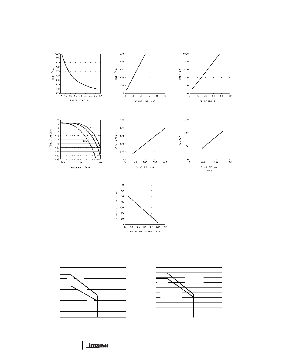
Typical Performance Curves
R
SET
vs
Horizontal Frequency
Back Porch Clamp
On Time vs R
SET
Vertical Default Delay
Time vs R
SET
Filter 3dB B
W
vs R
F
Level Out (Pin 9) vs
Sync. Tip Amplitude
Minimum Signal Detect
vs R
LV
Filter Attenuation vs R
F
@
f = 3.58MHz
Note 1: For R
LV
< 1000k
, no signal detect output (pin 10) will default high at
minimum signal sensitivity specification, or at complete loss of signal.
Package Power Dissipation vs Ambient Temperature
JEDEC JESD51-3 Low Effective Thermal Conductivity
Test Board
1.8
1.6
1.4
1.2
1
0.8
0.6
0.4
0.2
0
0
25
50
75
100
125
150
Ambient Temperature (∞C)
P
o
we
r
Di
ss
i
p
ati
o
n
(W
)
85
1.54W
PD
IP1
6
JA =8
1∞C
/W
1.136W
SO1
6 (0.1
50")
JA=11
0∞C
/W
2
1.8
1.6
1.4
1.2
1
0.8
0.4
0.2
0
P
o
we
r
Di
ss
i
p
ati
o
n
(W
)
0.6
0
25
50
75
100
125
150
Ambient Temperature (∞C)
Package Power Dissipation vs Ambient Temperature
JEDEC JESD51-7 High Effective Thermal Conductivity
Test Board
1.786W
1.563W
SO16 (0.150")
JA
=80∞C/W
PDIP16
JA
=70∞C/W
EL4583

5
Timing Diagram
Notes:
b. The composite sync output reproduces all the video input sync pulses, with a propagation delay.
c. Vertical sync leading edge is coincident with the first vertical serration pulse leading edge, with a propagation delay.
d. Odd-even output is low for even field, and high for odd field.
e. Back porch goes low for a fixed pulse width on the trailing edge of video input sync pulses. Note that for serration pulses during
vertical, the back porch starts on the rising edge of the serration pulse (with propagation delay).
f. Horizontal sync output produces the true "H" pulses of nominal width of 5µs. It has the same delay as the composite sync.
FIGURE 1.
EL4583