1
Æ
FN6167.0
EL5000A
High Voltage TFT-LCD Logic Driver
The EL5000A is high voltage TFT-LCD logic driver with
+40V and -30V output swing capability. Manufactured using
the Intersil proprietary monolithic high voltage bipolar
process, it is capable of delivering 100mA output peak
current into 5nF of capacitive load. To simplify external
circuitry, the EL5000A integrates additional logic circuits.
The EL5000A can operate on 3.3V logic supply and high
voltage -30V to +40V output supplies. The EL5000A is
available in TSSOP-16 package. It is specified for operation
over the -20∞C to +85∞C extended temperature range.
Features
∑ 3.3V logic supply
∑ 40V V
ON
output high level
∑ -30V V
OFF
output low level
∑ 166kHz input logic frequency
∑ 100mA output peak current
∑ 10mA output continuous current
∑ TTL-compatible logic input
∑ Pb-free plus anneal available (RoHS compliant)
Applications
∑ TFT-LCD panels
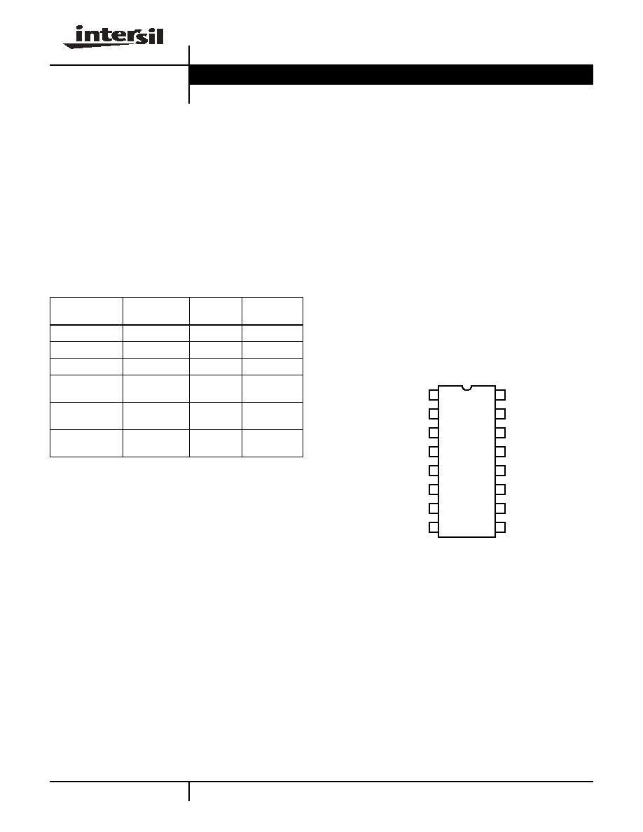
Pinout
EL5000A
(16-PIN TSSOP)
TOP VIEW
Ordering Information
PART
NUMBER
PACKAGE
TAPE &
REEL
PKG. DWG. #
EL5000AER
16-Pin TSSOP
-
MDP0044
EL5000AER-T7
16-Pin TSSOP
7"
MDP0044
EL5000AER-T13
16-Pin TSSOP
13"
MDP0044
EL5000AERZ
(See Note)
16-Pin TSSOP
(Pb-Free)
-
MDP0044
EL5000AERZ-T7
(See Note)
16-Pin TSSOP
(Pb-Free)
7"
MDP0044
EL5000AERZ-
T13 (See Note)
16-Pin TSSOP
(Pb-Free)
13"
MDP0044
NOTE: Intersil Pb-free plus anneal products employ special Pb-free
material sets; molding compounds/die attach materials and 100%
matte tin plate termination finish, which are RoHS compliant and
compatible with both SnPb and Pb-free soldering operations. Intersil
Pb-free products are MSL classified at Pb-free peak reflow
temperatures that meet or exceed the Pb-free requirements of
IPC/JEDEC J STD-020.
1
2
3
4
16
15
14
13
5
6
7
12
11
10
8
9
VON1
CKV
CKVCS
NC
CKVBCS
CKVB
STVP
VOFF
VDD
DISH
OECON
GND
STV
OE
CPV
GND
Data Sheet
July 28, 2005
CAUTION: These devices are sensitive to electrostatic discharge; follow proper IC Handling Procedures.
1-888-INTERSIL or 1-888-468-3774
|
Intersil (and design) is a registered trademark of Intersil Americas Inc.
Copyright Intersil Americas Inc. 2005. All Rights Reserved
All other trademarks mentioned are the property of their respective owners.

2
FN6167.0
July 28, 2005
IMPORTANT NOTE: All parameters having Min/Max specifications are guaranteed. Typical values are for information purposes only. Unless otherwise noted, all tests
are at the specified temperature and are pulsed tests, therefore: T
J
= T
C
= T
A
Absolute Maximum Ratings
(T
A
= 25∞C)
V
DD
. . . . . . . . . . . . . . . . . . . . . . . . . . . . . . . . . . . . . . . . . . . . . . 4.5V
V
ON
. . . . . . . . . . . . . . . . . . . . . . . . . . . . . . . . . . . . . . . . . . . . . . .44V
V
OFF
. . . . . . . . . . . . . . . . . . . . . . . . . . . . . . . . . . . . . . . . . . . . . -33V
V
CL
. . . . . . . . . . . . . . . . . . . . . . . . . . . . . . . . . . . . . . . . . . . . . . 4.5V
V
CKV
, V
CKVB
, V
STVP
,
V
CKVCS
, V
CKVBCS
, V
STVP
. . . . . . . . V
ON
+ 1 diode/V
OFF
- 1 diode
V
CPV
, V
OE
, V
STV
, V
OECON
. . . . . . . V
DD
+ 1 diode/GND - 1 diode
V
DISH
. . . . . . . . . . . . . . . . . . . . . . . GND + 1 diode/V
OFF
- 1 diode
I
OUT
(peak) . . . . . . . . . . . . . . . . . . . . . . . . . . . . . . . . . . . . . . 100mA
I
OUT
(continuos), CKV, CKVB, or STVP . . . . . . . . . . . . . . . . . 30mA
I
OUT
(continuous, total) . . . . . . . . . . . . . . . . . . . . . . . . . . . . . . 50mA
T
AMBIENT
. . . . . . . . . . . . . . . . . . . . . . . . . . . . . . . . .-20∞C to +85∞C
T
JUNCTION
. . . . . . . . . . . . . . . . . . . . . . . . . . . . . . .-20∞C to +150∞C
T
STORAGE
. . . . . . . . . . . . . . . . . . . . . . . . . . . . . . . .-65∞C to +150∞C
P
DISSIPATION
. . . . . . . . . . . . . . . . . . . . . . . . . . . . . . . . See Curves
Maximum Power Dissipation . . . . . . . . . . . . . . . . . . . . . See Curves
CAUTION: Stresses above those listed in "Absolute Maximum Ratings" may cause permanent damage to the device. This is a stress only rating and operation of the
device at these or any other conditions above those indicated in the operational sections of this specification is not implied.
Electrical Specifications
V
ON
= 20V, V
OFF
= -14V, V
DD
= 3.3V, 4.7nF Load on STV, CKV, CKVB, unless otherwise specified.
PARAMETER
DESCRIPTION
CONDITION
MIN
TYP
MAX
UNIT
I
VDD
V
DD
Supply Current
All inputs low
1.1
mA
CPV = 3.1V, other inputs low
0.7
1.5
2.5
mA
I
VON
V
ON
Supply Current
All inputs low
0.25
mA
CPV = 3.1V, other inputs low
0.2
0.45
0.9
mA
I
VOFF
V
OFF
Supply Current
All inputs low
0.25
mA
CPV = 3.1V, other inputs low
-1.25
-0.7
-0.30
mA
I
STV
STV Input Current
STV = 3.1V
25
130
180
µA
STV = 0.2V
-1
0
1
µA
I
CPV
CPV Input Current
CPV = 3.1V
20
60
90
µA
CPV = 0.2V
-1
0
1
µA
I
OE
OE Input Current
OE = 0.2V
-1
0
1
µA
OE = 3.1V, OECON = 0.2V
200
450
700
µA
OE = 3.1V, OECON = 3.1V
-1
0
1
µA
I
OECON
OECON Input Current
OECON - 0.2V, OE = 3.1V
-40
-25
-5
µA
OECON - 0.2V, OE = 0.2V
-1
0
1
µA
V
CKV
+
CKV Positive Output Swing
V
ON
= +20V, 1mA output current
19.1
19.3
19.5
V
V
CKV
CKV Negative Output Swing
V
OFF
= -14V, 1mA output current
-13.1
-13.3
-13.5
V
V
CKVB
+
CKVB Positive Output Swing
V
ON
= +20V, 1mA output current
19.1
19.3
19.5
V
V
CKVB
CKVB Negative Output Swing
V
OFF
= -14V, 1mA output current
-13.1
-13.3
-13.5
V
V
STVP
+
STVP Positive Output Swing
V
ON
= +20V, 1mA output current
19.0
19.2
19.4
V
V
STVP
STVP Negative Output Swing
V
OFF
= -14V, 1mA output current
-13.1
-13.3
-13.5
V
R
IN
CPV, OE, STV Input Resistance
3
k
C
IN
CPV, OE, STV Input Capacitance
1.5
pF
T
R
-CKV
CKV Rise Time
0.3
0.5
0.7
µs
T
F
-CKV
CKV Fall Time
0.5
0.75
1
µs
T
R
-CKVB
CKVB Rise Time
0.3
0.5
0.7
µs
T
F
-CKVB
CKVB Fall Time
0.5
0.75
1
µs
T
R
-STVP
STVP Rise Time
1.2
1.6
2.4
µs
T
F
-STVP
STVP Fall Time
1.2
1.6
2.4
µs
EL5000A
3
FN6167.0
July 28, 2005
T
D
-CKV+
CKV Rising Edge Delay Time
0.5
0.9
1.3
µs
T
D
-CKV-
CKV Falling Edge Delay Time
0.7
1.1
1.5
µs
T
D
-CKVB+
CKVB Rising Edge Delay Time
0.5
0.9
1.3
µs
T
D
-CKVB-
CKVB Falling Edge Delay Time
0.7
1.1
1.5
µs
T
D
-STVP+
STVP Rising Edge Delay Time
1.3
1.75
2.2
µs
T
D
-STVP-
STVP Falling Edge Delay Time
1.2
1.7
2
µs
T
D
-CKV_CS+
CKV_CS Rising Edge Delay Time
1.6
2.3
2.9
µs
T
D
-CKV_CS-
CKV_CS Falling Edge Delay Time
3.4
4.1
4.8
µs
T
D
-CKVB_CS+ CKVB_CS Rising Edge Delay Time
1.6
2.3
2.9
µs
T
D
-CKVB_CS-
CKVB_CS Falling Edge Delay Time
3.4
4.1
4.8
µs
Electrical Specifications
V
ON
= 20V, V
OFF
= -14V, V
DD
= 3.3V, 4.7nF Load on STV, CKV, CKVB, unless otherwise specified.
(Continued)
PARAMETER
DESCRIPTION
CONDITION
MIN
TYP
MAX
UNIT
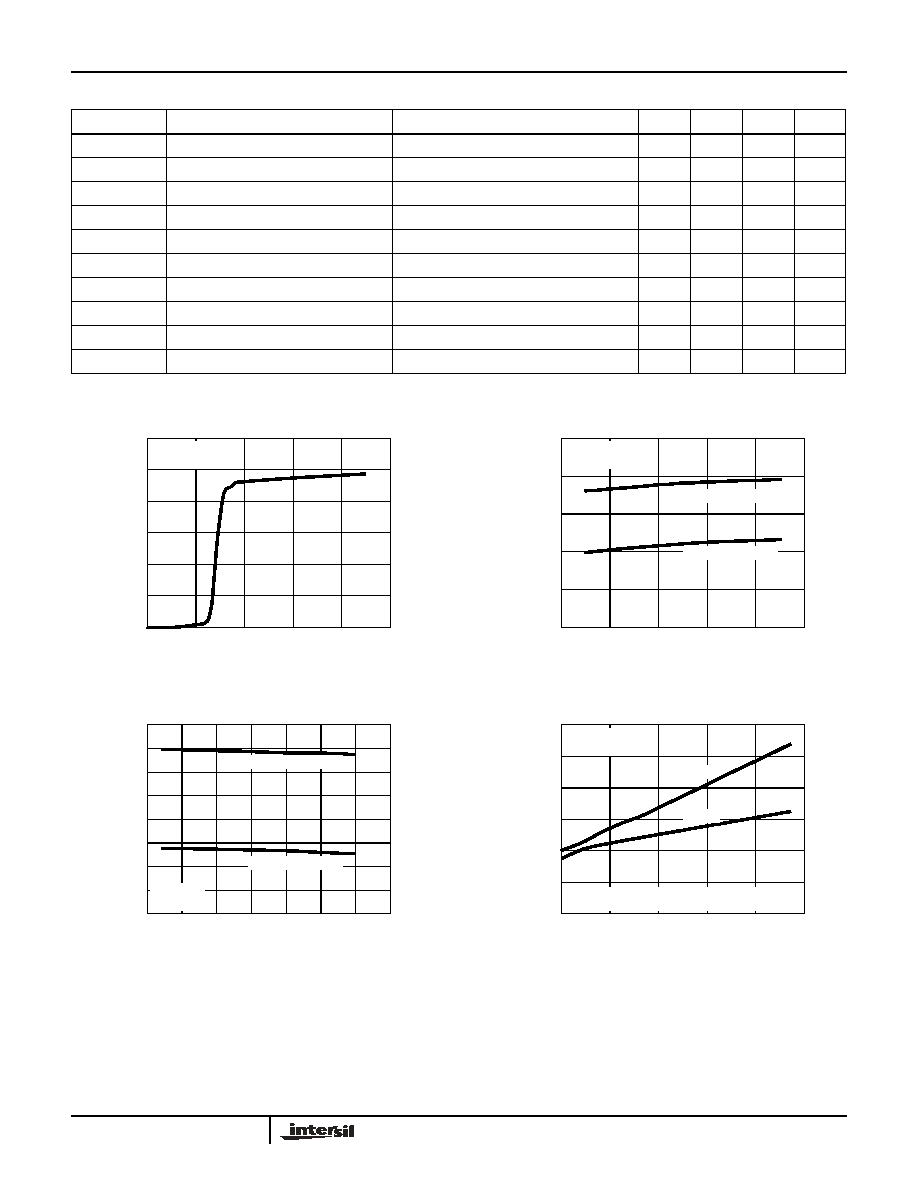
Typical Performance Curves
FIGURE 1. V
SS
SUPPLY CURRENT vs V
CC
FIGURE 2. V
ON
DC SUPPLY CURRENT vs V
ON
FIGURE 3. V
OFF
DC SUPPLY CURRENT vs V
OFF
FIGURE 4. CLOCK DELAY vs LOAD CAPACITOR
V
ON
=20V
V
OFF
=-14V
I
VCC
(m
A
)
1.5
1.25
1
0.75
0.5
0.25
0
0
1
2
3
4
5
V
CC
(V)
CPV INPUT HIGH
V
CC
=3.3V
V
OFF
=-14V
ALL INPUTS LOW
I
VON
(µA)
500
400
300
200
100
0
0
10
20
30
40
50
V
ON
(V)
CPV INPUT HIGH
ALL INPUTS LOW
V
CC
=3.3V
V
ON
=20V
I
VO
FF
(µA)
800
600
400
200
0
-35
-30
-25
-20
-10
0
V
OFF
(V)
-15
-5
FALL
DELAY FROM CPV INPUT TO CKV OR
CKVB REACHING 50% OF FINAL VALUE
DE
L
A
Y
(
µ
s
)
1.5
1.25
1
0.75
0.5
0.25
0
0
1K
2K
3K
4K
5K
LOAD CAPACITANCE (pF)
V
ON
=20V
V
OFF
=-14V
RISE
EL5000A

4
FN6167.0
July 28, 2005
FIGURE 5. CLOCK DELAY vs LOAD CAPACITOR
FIGURE 6. CLOCK DELAY vs TEMPERATURE
FIGURE 7. V
CC
SUPPLY CURRENT vs TEMPERATURE
FIGURE 8. DC SUPPLY CURRENTS vs TEMPERATURE
FIGURE 9. INPUT BIAS CURRENTS vs TEMPERATURE
FIGURE 10. OUTPUT SWING HEADROOM vs TEMPERATURE
Typical Performance Curves
(Continued)
FALL
DELAY FROM CPV INPUT TO CKV OR
CKVB REACHING 50% OF FINAL VALUE
DELAY (
µ
s)
1.5
1.25
1
0.75
0.5
0.25
0
0
1K
2K
3K
4K
5K
LOAD CAPACITANCE (pF)
V
ON
=40V
V
OFF
=-20V
RISE
FALL
4.7nF LOAD CAPACITORS
DELAY (
µ
s)
1.5
1.25
1
0.75
0.5
0.25
0
-25
25
75
125
AMBIENT TEMPERATURE (∞C)
V
ON
=20V
V
OFF
=-14V
RISE
I
VCC
(m
A
)
1.4
1.2
1
0.8
0.6
-25
25
75
125
AMBIENT TEMPERATURE (∞C)
V
CC
=3.3V
V
ON
=20V
V
OFF
=-14V
S
U
P
P
LY CURR
E
N
T
(µA)
1K
800
400
200
0
-25
25
75
125
AMBIENT TEMPERATURE (∞C)
V
CC
=3.3V
V
ON
=20V
V
OFF
=-14V
600
I
VOFF
, CPV HIGH
I
VOFF
, INPUTS LOW
I
VON
, CPV HIG
H
I
VON
, INPUTS LOW
INPUT CU
RRE
N
T
(µA)
500
300
100
-100
-25
25
75
125
AMBIENT TEMPERATURE (∞C)
400
200
0
OE INPUT, 3.3V
STV INPUT, 3.3V
CPV INPUT, 3.3V
OECON INPUT, 0.2V
HEADROOM (
m
V)
750
500
250
0
-25
25
75
125
AMBIENT TEMPERATURE (∞C)
CKV, CKVB, AND STVP OUTPUTS
5mA LOAD
EL5000A

5
FN6167.0
July 28, 2005
FIGURE 11. POWER CONSUMPTION vs FREQUENCY AND
LOAD
FIGURE 12. POWER CONSUMPTION vs FREQUENCY AND
LOAD
FIGURE 13. PACKAGE POWER DISSIPATION vs AMBIENT
TEMPERATURE
FIGURE 14. PACKAGE POWER DISSIPATION vs AMBIENT
TEMPERATURE
Typical Performance Curves
(Continued)
V
ON
=40V
V
OFF
=-20V
R
CS
=500
P
O
WER DI
SSI
PATIO
N
(
m
W)
1400
800
400
0
0
0
100
200
INPUT FREQUENCY (kHz)
1200
600
200
150
1000
4700pF
1000pF
220pF
V
ON
=20V
V
OFF
=-14V
R
CS
=500
P
O
WER DI
SSI
PATIO
N
(
m
W)
800
0
0
0
100
200
INPUT FREQUENCY (kHz)
600
200
150
400
4700pF
1000pF
220pF
JEDEC JESD51-3 LOW EFFECTIVE THERMAL
CONDUCTIVITY TEST BOARD
845mW
TSS
OP
16
JA
=14
8∞C
/W
P
O
WER DIS
S
IPATION
(W)
1.2
0.8
0.4
0
0
25
75
150
AMBIENT TEMPERATURE (∞C)
0.6
0.2
125
1
50
100
85
JEDEC JESD51-7 HIGH EFFECTIVE THERMAL
CONDUCTIVITY TEST BOARD
1.289W
TSS
OP
16
JA
=97
∞C/W
P
O
WER DIS
S
IPATION
(W)
1.8
1.2
0.4
0
0
25
75
150
AMBIENT TEMPERATURE (∞C)
0.8
0.2
125
1.6
50
100
85
1
0.6
1.4
EL5000A