Äîêóìåíòàöèÿ è îïèñàíèÿ www.docs.chipfind.ru
1
®
FN7376.2
CAUTION: These devices are sensitive to electrostatic discharge; follow proper IC Handling Procedures.
1-888-INTERSIL or 321-724-7143
|
Intersil (and design) is a registered trademark of Intersil Americas Inc.
Copyright © Intersil Americas Inc. 2004, 2005. All Rights Reserved.
All other trademarks mentioned are the property of their respective owners.
EL5001
6-Channel Clock Driver
The EL5001 is a 6-channel level shifting driver designed
primarily for use as a clock driver in LTPS LCD displays. The
EL5001 buffers and level shifts six logic level input signals.
The six channels are grouped in to two sets, one of two
channels and one of four channels. Each set can be
configured in the inverting or non-inverting modes.
Operating from 3.3V input logic, the output swing is set using
two reference input pins. These pins can be up to 18V
differential and are not buffered, so should therefore be
bypassed effectively.
The EL5001 is designed to drive capacitive loads of 500pF
with rise and fall times of just 20ns. A three-state pin is
provided to set all outputs in to a high impedance mode. The
ENABLE pin can be used to put the device in to a power
save mode where the power consumption drops to just 3µA.
The EL5001 is available in 20-pin QFN (4mm x 4mm) and
HTSSOP packages. Both are specified for operation over
the -40°C to +85°C temperature range.
Features
· SIx inverting/non-inverting channels
· 3.3V input logic
· 18V output
· 250µA typical supply current
· Drives up to 500pF
· T
R
/T
F
= 35ns max
· Disable function
· 20-pin QFN (4mm x 4mm) and HTSSOP packages
· Pb-free available (RoHS compliant)
Applications
· LTPS LCD clock drivers
· CCD driving
· Level shifters
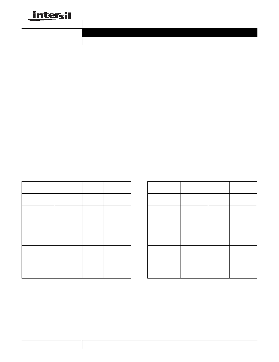
Ordering Information
PART NUMBER
PACKAGE
TAPE &
REEL
PKG. DWG. #
PART NUMBER
PACKAGE
TAPE &
REEL
PKG. DWG. #
EL5001IL
20-Pin QFN
(4mm x 4mm)
-
MDP0046
EL5001IRE
20-Pin
HTSSOP
-
MDP0048
EL5001IL-T7
20-Pin QFN
(4mm x 4mm)
7"
MDP0046
EL5001IRE-T7
20-Pin
HTSSOP
7"
MDP0048
EL5001IL-T13
20-Pin QFN
(4mm x 4mm)
13"
MDP0046
EL5001IRE-T13
20-Pin
HTSSOP
13"
MDP0048
EL5001ILZ
(See Note)
20-Pin QFN
(4mm x 4mm)
(Pb-Free)
-
MDP0046
EL5001IREZ
(See Note)
20-Pin
HTSSOP
(Pb-Free)
-
MDP0048
EL5001ILZ-T7
(See Note)
20-Pin QFN
(4mm x 4mm)
(Pb-Free)
7"
MDP0046
EL5001IREZ-T7
(See Note)
20-Pin
HTSSOP
(Pb-Free)
7"
MDP0048
EL5001ILZ-T13
(See Note)
20-Pin QFN
(4mm x 4mm)
(Pb-Free)
13"
MDP0046
EL5001IREZ-T13
(See Note)
20-Pin
HTSSOP
(Pb-Free)
13"
MDP0048
NOTE: Intersil Pb-free products employ special Pb-free material sets; molding compounds/die attach materials and 100% matte tin plate termination
finish, which are RoHS compliant and compatible with both SnPb and Pb-free soldering operations. Intersil Pb-free products are MSL classified at Pb-
free peak reflow temperatures that meet or exceed the Pb-free requirements of IPC/JEDEC J STD-020C.
Data Sheet
January 31, 2005
2
FN7376.2
January 31, 2005
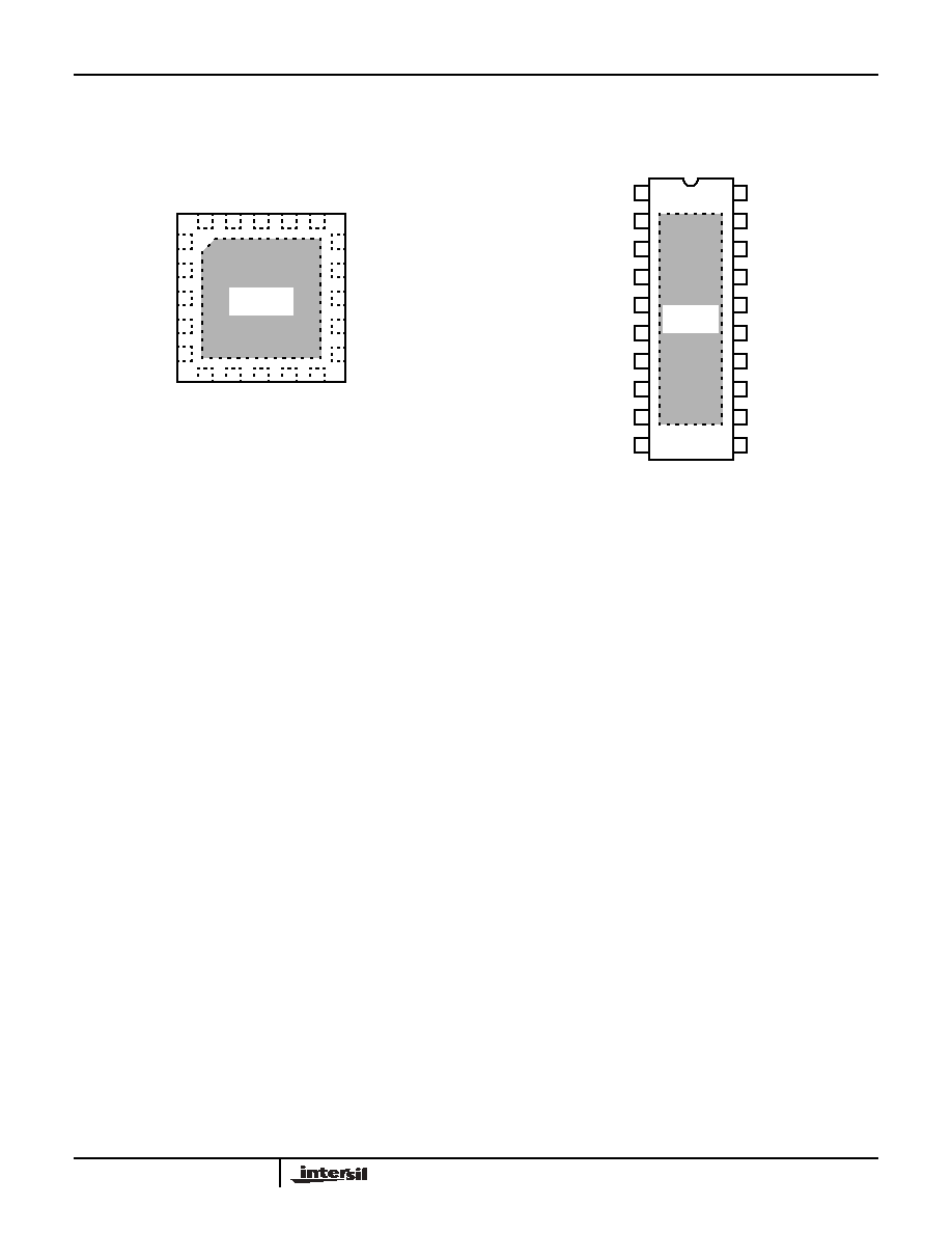
Pinouts
EL5001
[20-PIN QFN (4mm x 4mm)]
TOP VIEW
EL5001
(20-PIN HSSOP)
TOP VIEW
1
2
3
4
15
14
13
12
6
7
8
9
20
19
18
17
IN1
IN2
IN3
IN4
IN6
INV
1
INV
2
VL
EN
TRI
GND
VH
OUT1
OUT2
OUT3
OUT4
THERMAL
PAD
5
IN5
10
OUT
6
11 OUT5
16
NC
1
2
3
4
16
15
14
13
5
6
7
12
11
9
8
10
20
19
18
17
TRI
EN
IN1
IN2
IN3
IN4
IN5
IN6
INV1
INV2
GND
VH
OUT1
OUT2
OUT3
OUT4
OUT5
OUT6
VL
NC
THERMAL
PAD
EL5001
3
FN7376.2
January 31, 2005
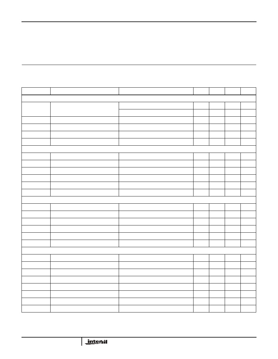
Absolute Maximum Ratings
(T
A
= 25°C)
Supply Voltage between V
SD
and GND . . . . . . . . . . . . . . . . . . .18V
Maximum Continuous Output Current . . . . . . . . . . . . . . . . . . . 50mA
Ambient Operating Temperature . . . . . . . . . . . . . . . .-40°C to +85°C
Maximum Die Temperature . . . . . . . . . . . . . . . . . . . . . . . . . . +125°C
Storage Temperature . . . . . . . . . . . . . . . . . . . . . . . .-65°C to +150°C
Power Dissipation . . . . . . . . . . . . . . . . . . . . . . . . . . . . . See Curves
CAUTION: Stresses above those listed in "Absolute Maximum Ratings" may cause permanent damage to the device. This is a stress only rating and operation of the
device at these or any other conditions above those indicated in the operational sections of this specification is not implied.
IMPORTANT NOTE: All parameters having Min/Max specifications are guaranteed. Typical values are for information purposes only. Unless otherwise noted, all tests
are at the specified temperature and are pulsed tests, therefore: T
J
= T
C
= T
A
Electrical Specifications
V
H
= 10V, V
L
= -5V, EN = 3V, unless otherwise specified
.
PARAMETER
DESCRIPTION
CONDITION
MIN
TYP
MAX
UNIT
POWER SUPPLY
I
S
Supply Current
EN = 3V, IN
X
= 0V
750
1200
µA
EN = 3V, IN
X
= 3V
250
500
µA
I
S_DIS
Supply Current - Disabled
EN = 0V, IN
X
= 0V
3
µA
V
LR
V
L
Range
-13
0
V
V
HR
V
H
Range
5
18
V
V
H
-V
L
Maximum V
H
- V
L
Range
0
18
V
INPUT
V
IH
Logic `1' Input Voltage
2.0
V
I
IH
Logic `1' Input Current
0.1
10
µA
V
IL
Logic `0' Input Voltage
0.8
V
I
IL
Logic `0' Input Current
0.1
10
µA
C
IN
Input Capacitance
3.5
pF
R
IN
Input Resistance
50
M
OUTPUT
V
OH
V
OUTL
High
IN
X
= 10V, I
L
= 10mA
9.80
9.88
V
V
OL
V
OUTL
Low
IN
X
= 0V, I
L
= -10mA
-4.90
-4.88
V
R
OH
On Resistance V
H
to OUT
I
L
= 50mA
11
15
R
OL
On Resistance V
L
to OUT
I
L
= 50mA
11
15
I
PEAK
Peak Output Current
500
mA
I
L
Out Leakage Current
0.1
0.5
µA
SWITCHING CHARACTERISTICS
t
R
Rise Time
C
L
= 500pF
20
35
ns
t
F
Fall Time
C
L
= 500pF
20
35
ns
t
RFD
T
R
, T
F
Matching
C
L
= 500pF
5
ns
t
D
+
Turn On Delay
C
L
= 500pF
55
ns
t
D
-
Turn Off Delay
C
L
= 500pF
55
ns
t
DD
t
D
+, t
D
-, Matching
C
L
= 500pF
5
ns
t
EN
Enable Time
9.8
µs
t
DIS
Disable Time
2.2
µs
EL5001
4
FN7376.2
January 31, 2005
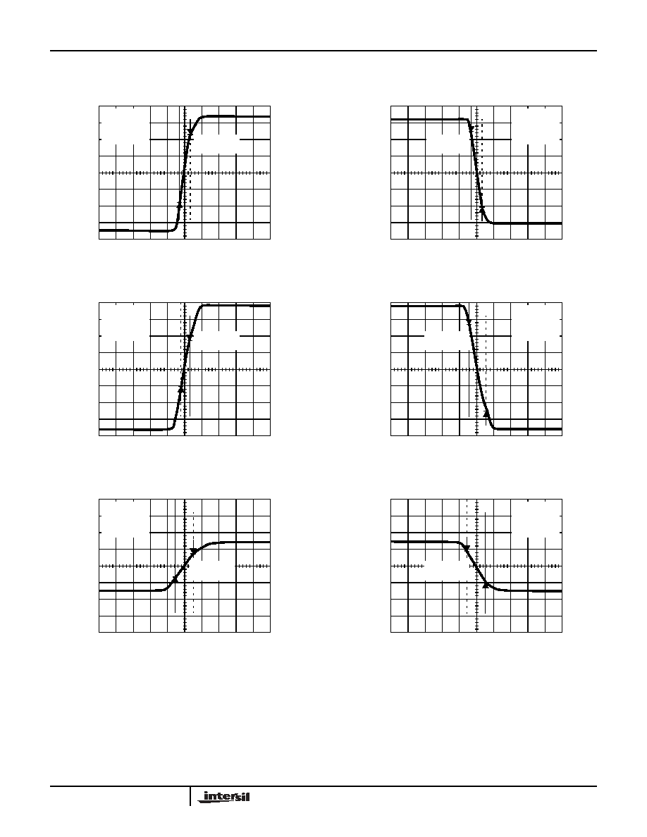
Typical Performance Curves
FIGURE 1. RISE TIME OUTPUT 6V
P-P
FIGURE 2. FALL TIME OUTPUT 6V
P-P
FIGURE 3. RISE TIME OUTPUT 12V
P-P
FIGURE 4. FALL TIME OUTPUT 12V
P-P
FIGURE 5. RISE TIME OUTPUT 5V
P-P
FIGURE 6. FALL TIME OUTPUT 5V
P-P
TIME (40ns/DIV)
VO
L
T
AG
E (1
V/
DI
V)
R
L
=0
C
L
=500pF
V
S
=V-=0V
V
S
=V+=18V
RISE TIME
T=37.55ns
TIME (40ns/DIV)
VO
L
T
AG
E (1
V/
DI
V)
R
L
=0
C
L
=500pF
V
S
=V-=0V
V
S
=V+=18V
FALL TIME
T=29ns
TIME (20ns/DIV)
V
O
L
T
AG
E (
2
V/
DI
V
)
R
L
=0
C
L
=500pF
V
S
=V-=0V
V
S
=V+=18V
RISE TIME
T=23.63ns
TIME (20ns/DIV)
V
O
L
T
AG
E (
2
V/
DI
V
)
R
L
=0
C
L
=500pF
V
S
=V-=0V
V
S
=V+=18V
FALL TIME
T=22.93ns
TIME (20ns/DIV)
VO
L
T
A
G
E
(2
V/
D
I
V)
R
L
=0
C
L
=500pF
V
S
=V-=0V
V
S
=V+=18V
RISE TIME
T=40.08ns
TIME (20ns/DIV)
VO
L
T
A
G
E
(2
V/
D
I
V)
R
L
=0
C
L
=500pF
V
S
=V-=0V
V
S
=V+=18V
FALL TIME
T=30.57ns
EL5001
5
FN7376.2
January 31, 2005
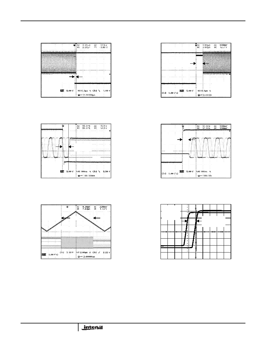
FIGURE 7. DISABLE RESPONSE
FIGURE 8. ENABLE RESPONSE
FIGURE 9. TURN-OFF (TRI)
FIGURE 10. TURN-ON (TRI)
FIGURE 11. ENABLE/DISABLE THRESHOLD
FIGURE 12. PROPAGATION DELAY
Typical Performance Curves
(Continued)
TIME (10µs/DIV)
V
O
L
T
A
G
E (
1
V/D
I
V
)
R
L
=0
C
L
=500pF
V
S
=V-=0V
V
S
=V+=18V
DISABLE
T=2.2µs
CH2
CH3
R
L
=0
C
L
=500pF
V
S
=V-=0V
V
S
=V+=18V
ENABLE
T=9.8µs
CH2
CH3
TIME (10µs/DIV)
V
O
L
T
A
G
E (
1
V/D
I
V
)
TURN-OFF
T=90ns
R
L
=0
C
L
=500pF
V
S
=V-=0V
V
S
=V+=18V
CH2
CH3
TIME (100ns/DIV)
V
O
L
T
A
GE
(CH1-
1
V
/
D
I
V
)
(
CH2-5
V/DIV)
TURN-ON
T=90ns
R
L
=0
C
L
=500pF
V
S
=V-=0V
V
S
=V+=18V
CH2
CH3
TIME (100ns/DIV)
V
O
L
T
A
GE
(CH1-
1
V
/
D
I
V
)
(
CH2-5
V/DIV)
GROUND
1.78V
1.32V
R
L
=0
C
L
=500pF
V
S
=V-=0V
V
S
=V+=18V
CH2
CH3
TIME (2µs/DIV)
V
O
L
T
A
G
E (
C
H
2
-
5
V/D
I
V)
(C
H
3
-1
V
/
D
I
V)
PROPAGATION
DELAY
T=52ns
R
L
=0
C
L
=500pF
V
S
=V-=0V
V
S
=V+=18V
TIME (40ns/DIV)
VO
L
T
AG
E (2
V/
DI
V)
EL5001