 | ÐлекÑÑоннÑй компоненÑ: EL5128CYZ | СкаÑаÑÑ:  PDF PDF  ZIP ZIP |
Äîêóìåíòàöèÿ è îïèñàíèÿ www.docs.chipfind.ru
1
®
FN7000.2
EL5128
Dual V
COM
Amplifier & Gamma Reference
Buffer
The EL5128 integrates two V
COM
amplifiers with a single gamma
reference buffer. Operating on
supplies ranging from 5V to 15V, while consuming only
2.0mA, the EL5128 has a bandwidth of 12MHz (-3dB) and
provides common mode input ability beyond the supply rails,
as well as rail-to-rail output capability. This enables the
amplifier to offer maximum dynamic range at any supply
voltage. The EL5128 also features fast slewing and settling
times, as well as a high output drive capability of 30mA (sink
and source).
The EL5128 is targeted at TFT-LCD applications, including
notebook panels, monitors, and LCD-TVs. It is available in
the 10-pin MSOP package and is specified for operation
over the -40°C to +85°C temperature range.
Pinout
EL5128
(10-PIN MSOP)
TOP VIEW
Features
· Dual V
COM
amplifier
· Single gamma reference buffer
· 12MHz -3dB bandwidth
· Supply voltage = 4.5V to 16.5V
· Low supply current = 2.0mA
· High slew rate = 10V/µs
· Unity-gain stable
· Beyond the rails input capability
· Rail-to-rail output swing
· Ultra-small package
· Pb-free available
Applications
· TFT-LCD drive circuits
· Notebook displays
· LCD desktop monitors
· LCD-TVs
VOUTB
VINB-
VINB+
VS-
VOUTC
VOUTA
VINA-
VINA+
VS+
VINC
- +
-
+
1
2
3
4
10
9
8
7
5
6
Ordering Information
PART
NUMBER
PACKAGE
TAPE & REEL PKG. DWG. #
EL5128CY
10-Pin MSOP
-
MDP0043
EL5128CY-T7
10-Pin MSOP
7"
MDP0043
EL5128CY-T13 10-Pin MSOP
13"
MDP0043
EL5128CYZ
(See Note)
10-Pin MSOP
(Pb-free)
-
MDP0043
EL5128CYZ-T7
(See Note)
10-Pin MSOP
(Pb-free)
7"
MDP0043
EL5128CYZ-
T13 (See Note)
10-Pin MSOP
(Pb-free)
13"
MDP0043
NOTE: Intersil Pb-free products employ special Pb-free material
sets; molding compounds/die attach materials and 100% matte tin
plate termination finish, which is compatible with both SnPb and
Pb-free soldering operations. Intersil Pb-free products are MSL
classified at Pb-free peak reflow temperatures that meet or exceed
the Pb-free requirements of IPC/JEDEC J Std-020B.
Data Sheet
July 26, 2004
CAUTION: These devices are sensitive to electrostatic discharge; follow proper IC Handling Procedures.
1-888-INTERSIL or 321-724-7143
|
Intersil (and design) is a registered trademark of Intersil Americas Inc.
Copyright © Intersil Americas Inc. 2003, 2004. All Rights Reserved. Elantec is a registered trademark of Elantec Semiconductor, Inc.
All other trademarks mentioned are the property of their respective owners.
2
IMPORTANT NOTE: All parameters having Min/Max specifications are guaranteed. Typ values are for information purposes only. Unless otherwise noted, all tests are at
the specified temperature and are pulsed tests, therefore: T
J
= T
C
= T
A
Absolute Maximum Ratings
(T
A
= 25°C)
Supply Voltage between V
S
+ and V
S
- . . . . . . . . . . . . . . . . . . . .+18V
Input Voltage . . . . . . . . . . . . . . . . . . . . . . . . . . V
S
- - 0.5V, V
S
+ 0.5V
Maximum Continuous Output Current . . . . . . . . . . . . . . . . . . 30mA
Maximum Die Temperature . . . . . . . . . . . . . . . . . . . . . . . . . . +125°C
Storage Temperature . . . . . . . . . . . . . . . . . . . . . . . . -65°C to +150°C
Ambient Operating Temperature . . . . . . . . . . . . . . . . -40°C to +85°C
Power Dissipation . . . . . . . . . . . . . . . . . . . . . . . . . . . . . See Curves
CAUTION: Stresses above those listed in "Absolute Maximum Ratings" may cause permanent damage to the device. This is a stress only rating and operation of the
device at these or any other conditions above those indicated in the operational sections of this specification is not implied.
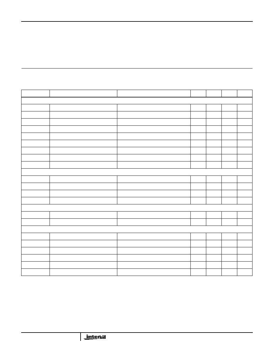
Electrical Specifications
V
S
+ = +5V, V
S
- = -5V, R
L
= 10k
and C
L
= 10pF to 0V, T
A
= 25°C unless otherwise specified
PARAMETER
DESCRIPTION
CONDITION
MIN
TYP
MAX
UNIT
INPUT CHARACTERISTICS
V
OS
Input Offset Voltage
V
CM
= 0V
2
12
mV
TCV
OS
Average Offset Voltage Drift
(Note 1)
5
µV/°C
I
B
Input Bias Current
V
CM
= 0V
2
50
nA
R
IN
Input Impedance
1
G
C
IN
Input Capacitance
1.35
pF
CMIR
Common-Mode Input Range
(V
COM
amps)
-5.5
+5.5
V
CMRR
Common-Mode Rejection Ratio
(V
COM
amps) for V
IN
from -5.5V to +5.5V
50
70
dB
A
VOL
Open-Loop Gain
-4.5V
V
OUT
+4.5V (V
COM
amps)
75
95
dB
AV
Voltage Gain
-4.5V
V
OUT
+4.5V
0.995
1.005
V/V
OUTPUT CHARACTERISTICS
V
OL
Output Swing Low
I
L
= -5mA
-4.92
-4.85
V
V
OH
Output Swing High
I
L
= 5mA
4.85
4.92
V
I
SC
Short Circuit Current
±120
mA
I
OUT
Output Current
±30
mA
POWER SUPPLY PERFORMANCE
PSRR
Power Supply Rejection Ratio
V
S
is moved from ±2.25V to ±7.75V
60
80
dB
I
S
Supply Current (per amplifier)
No load
660
1000
µA
DYNAMIC PERFORMANCE
SR
Slew Rate (Note 2)
-4.0V
V
OUT
+4.0V, 20% to 80%
10
V/µs
t
S
Settling to +0.1% (A
V
= +1)
(A
V
= +1), V
O
= 2V step
500
ns
BW
-3dB Bandwidth
R
L
= 10k
, C
L
= 10pF
12
MHz
GBWP
Gain-Bandwidth Product
R
L
= 10k
, C
L
= 10pF (V
COM
amps)
8
MHz
PM
Phase Margin
R
L
= 10k
, C
L
= 10pF (V
COM
amps)
50
°
CS
Channel Separation
f = 5MHz
75
dB
NOTES:
1. Measured over operating temperature range.
2. Slew rate is measured on rising and falling edges.
EL5128

3
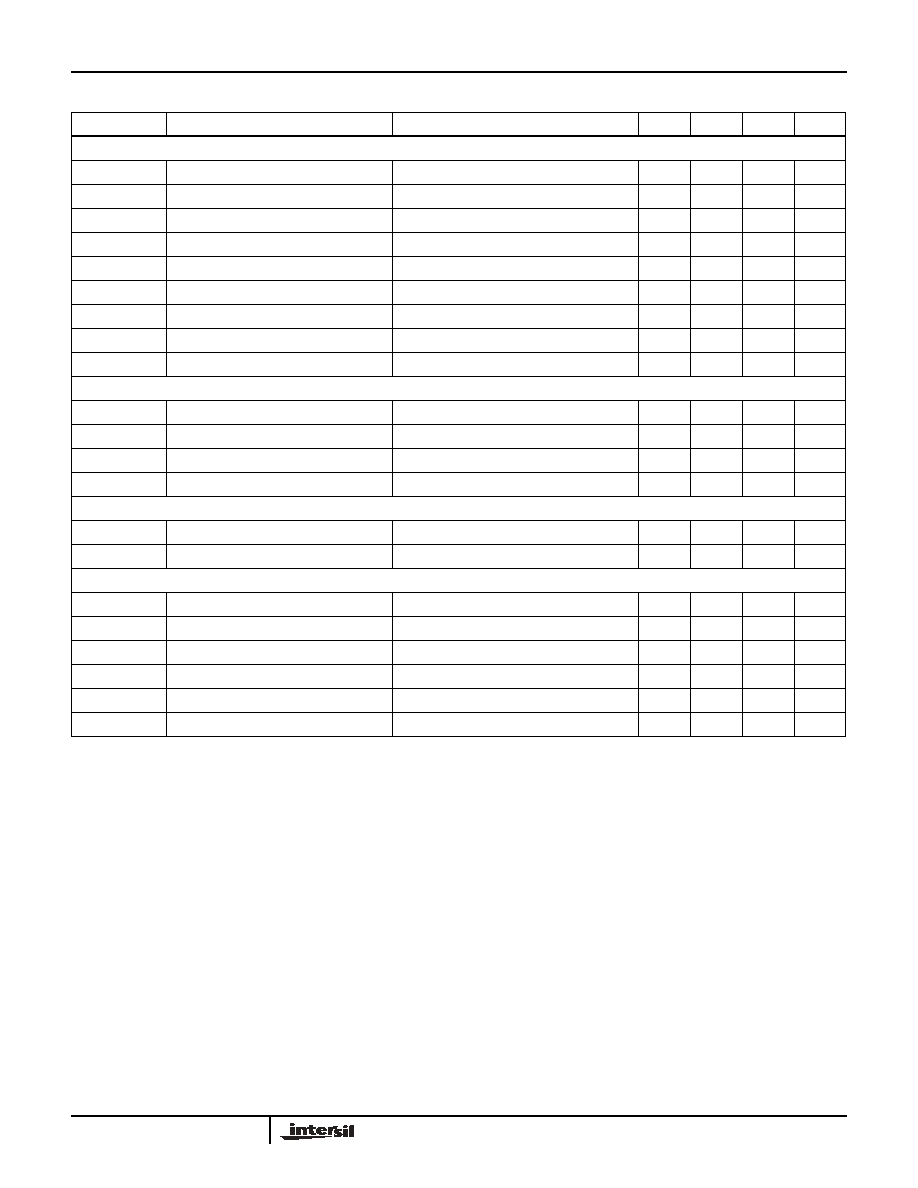
Electrical Specifications
V
S
+ = +5V, V
S
- = 0V, R
L
= 10k
and C
L
= 10pF to 2.5V, T
A
= 25°C unless otherwise specified
PARAMETER
DESCRIPTION
CONDITION
MIN
TYP
MAX
UNIT
INPUT CHARACTERISTICS
V
OS
Input Offset Voltage
V
CM
= 2.5V
2
10
mV
TCV
OS
Average Offset Voltage Drift
(Note 1)
5
µV/°C
I
B
Input Bias Current
V
CM
= 2.5V
2
50
nA
R
IN
Input Impedance
1
G
C
IN
Input Capacitance
1.35
pF
CMIR
Common-Mode Input Range
-0.5
+5.5
V
CMRR
Common-Mode Rejection Ratio
for V
IN
from -0.5V to +5.5V
45
66
dB
A
VOL
Open-Loop Gain
0.5V
V
OUT
+ 4.5V
75
95
dB
A
V
Voltage Gain
0.5V
V
OUT
+ 4.5V
0.995
1.005
V/V
OUTPUT CHARACTERISTICS
V
OL
Output Swing Low
I
L
= -5mA
80
150
mV
V
OH
Output Swing High
I
L
= +5mA
4.85
4.92
V
I
SC
Short Circuit Current
±120
mA
I
OUT
Output Current
±30
mA
POWER SUPPLY PERFORMANCE
PSRR
Power Supply Rejection Ratio
V
S
is moved from 4.5V to 15.5V
60
80
dB
I
S
Supply Current (per amplifier)
No load
660
1000
µA
DYNAMIC PERFORMANCE
SR
Slew Rate (Note 2)
1V
V
OUT
4V, 20% to 80%
10
V/µs
t
S
Settling to +0.1% (A
V
= +1)
(A
V
= +1), V
O
= 2V step
500
ns
BW
-3dB Bandwidth
R
L
= 10k
, C
L
= 10pF
12
MHz
GBWP
Gain-Bandwidth Product
R
L
= 10k
, C
L
= 10pF
8
MHz
PM
Phase Margin
R
L
= 10k
, C
L
= 10pF
50
°
CS
Channel Separation
f = 5MHz
75
dB
NOTES:
1. Measured over operating temperature range.
2. Slew rate is measured on rising and falling edges.
EL5128
4
Electrical Specifications
V
S
+ = +15V, V
S
- = 0V, R
L
= 10k
and C
L
= 10pF to 7.5V, T
A
= 25°C unless otherwise specified
PARAMETER
DESCRIPTION
CONDITION
MIN
TYP
MAX
UNIT
INPUT CHARACTERISTICS
V
OS
Input Offset Voltage
V
CM
= 7.5V
2
14
mV
TCV
OS
Average Offset Voltage Drift
(Note 1)
5
µV/°C
I
B
Input Bias Current
V
CM
= 7.5V
2
50
nA
R
IN
Input Impedance
1
G
C
IN
Input Capacitance
1.35
pF
CMIR
Common-Mode Input Range
-0.5
+15.5
V
CMRR
Common-Mode Rejection Ratio
for V
IN
from -0.5V to +15.5V
53
72
dB
A
VOL
Open-Loop Gain
0.5V
V
OUT
14.5V
75
95
dB
A
V
Voltage Gain
0.5V
V
OUT
14.5V
0.995
1.005
V/V
OUTPUT CHARACTERISTICS
V
OL
Output Swing Low
I
L
= -5mA
80
150
mV
V
OH
Output Swing High
I
L
= +5mA
14.85
14.92
V
I
SC
Short Circuit Current
±120
mA
I
OUT
Output Current
±30
mA
POWER SUPPLY PERFORMANCE
PSRR
Power Supply Rejection Ratio
V
S
is moved from 4.5V to 15.5V
60
80
dB
I
S
Supply Current (per amplifier)
No load
660
1000
µA
DYNAMIC PERFORMANCE
SR
Slew Rate (Note 2)
1V
V
OUT
14V, 20% to 80%
10
V/µs
t
S
Settling to +0.1% (A
V
= +1)
(A
V
= +1), V
O
= 2V step
500
ns
BW
-3dB Bandwidth
R
L
= 10k
, C
L
= 10pF
12
MHz
GBWP
Gain-Bandwidth Product
R
L
= 10k
, C
L
= 10pF
8
MHz
PM
Phase Margin
R
L
= 10k
, C
L
= 10pF
50
°
CS
Channel Separation
f = 5MHz
75
dB
NOTES:
1. Measured over operating temperature range.
2. Slew rate is measured on rising and falling edges.
EL5128
5
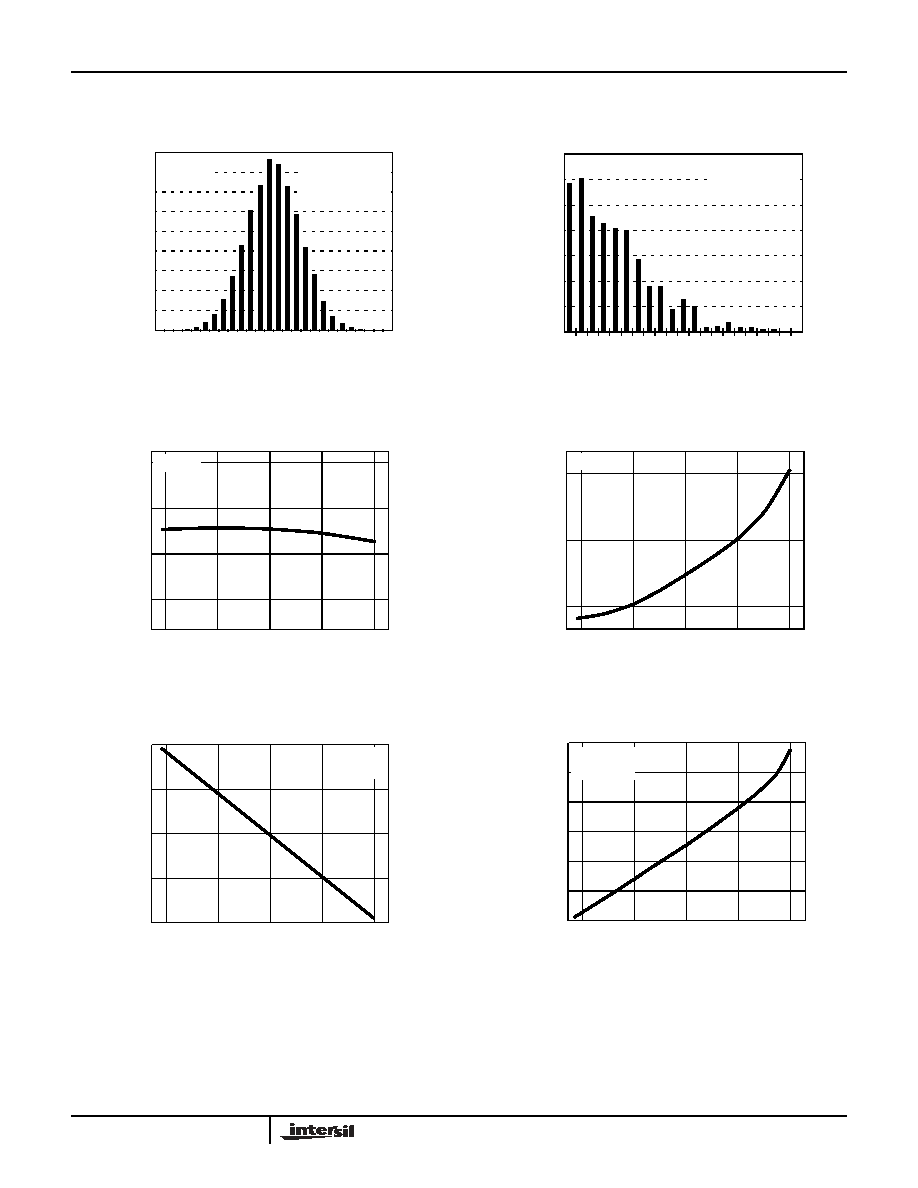
Typical Performance Curves
FIGURE 1. INPUT OFFSET VOLTAGE DISTRIBUTION
FIGURE 2. INPUT OFFSET VOLTAGE DRIFT
FIGURE 3. INPUT OFFSET VOLTAGE vs TEMPERATURE
FIGURE 4. INPUT BIAS CURRENT vs TEMPERATURE
FIGURE 5. OUTPUT HIGH VOLTAGE vs TEMPERATURE
FIGURE 6. OUTPUT LOW VOLTAGE vs TEMPERATURE
400
1200
QUANTITY (AMPLIFIE
R
S
)
INPUT OFFSET VOLTAGE (mV)
0
-12
1800
1600
800
200
1400
1000
600
-10
-8
-6
-4
-2
-0
2
4
6
8
10
12
V
S
=±5V
T
A
=25°C
TYPICAL
PRODUCTION
DISTRIBUTION
INPUT OFFSET VOLTAGE DRIFT, TCV
OS
(µV/°C)
1
3
5
7
9
11
13
15
17
19
21
10
50
QUANT
ITY (AMPLIF
I
ERS
)
0
70
30
60
40
20
V
S
=±5V
TYPICAL
PRODUCTION
DISTRIBUTION
0
150
0
5
INPUT OFFSET VO
LTAGE
(
m
V)
DIE TEMPERATURE (°C)
-5
50
-50
100
10 V
S
=±5V
0.0
INPUT
BIAS C
URRE
N
T
(nA)
DIE TEMPERATURE (°C)
-2.0
2.0
0
150
50
-50
100
V
S
=±5V
4.94
4.95
OUTPUT HIGH
VOL
T
AGE
(
V
)
4.93
4.97
0
150
DIE TEMPERATURE (°C)
50
-50
100
4.96
V
S
=±5V
I
OUT
=5mA
-4.95
-4.93
O
U
TPUT LOW VO
LTAG
E
(V)
-4.97
-4.91
0
150
DIE TEMPERATURE (°C)
50
-50
100
-4.92
-4.94
-4.96
V
S
=±5V
I
OUT
=-5mA
EL5128