Äîêóìåíòàöèÿ è îïèñàíèÿ www.docs.chipfind.ru
1
®
FN7383.2
CAUTION: These devices are sensitive to electrostatic discharge; follow proper IC Handling Procedures.
1-888-INTERSIL or 1-888-468-3774
|
Intersil (and design) is a registered trademark of Intersil Americas Inc.
Copyright © Intersil Americas Inc. 2003-2005. All Rights Reserved.
All other trademarks mentioned are the property of their respective owners.
EL5134, EL5135, EL5234, EL5235
650MHz, Gain of 5, Low Noise Amplifiers
The EL5134, EL5135, EL5234, and EL5235 are ultra-low
voltage noise, high speed voltage feedback amplifiers that
are ideal for applications requiring low voltage noise,
including communications and imaging. These devices offer
extremely low power consumption for exceptional noise
performance. Stable at gains as low as 5, these devices offer
100mA of drive performance. Not only do these devices find
perfect application in high gain applications, they maintain
their performance down to lower gain settings.
These amplifiers are available in small package options
(SOT-23) as well as the MSOP and the industry-standard
SO packages. All parts are specified for operation over the
-40°C to +85°C temperature range.
Features
· 650MHz -3dB bandwidth
· Ultra low noise 1.9nV/
Hz
· 450V/µs slew rate
· Low supply current = 7.3mA
· Single supplies from 5V to 12V
· Dual supplies from ±2.5V to ±5V
· Fast disable on the EL5134 and EL5234
· Duals EL5234 and EL5235
· Low cost
· Pb-free plus anneal available (RoHS compliant)
Applications
· Imaging
· Instrumentation
· Communications devices
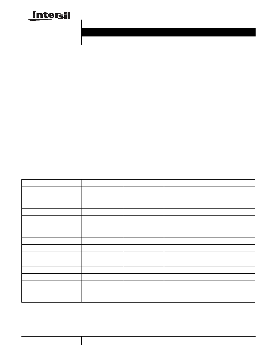
Ordering Information
PART NUMBER
PART MARKING
TAPE & REEL
PACKAGE
PKG. DWG. #
EL5134IS
5134IS
-
8 Ld SO
MDP0027
EL5134IS-T7
5134IS
7"
8 Ld SO
MDP0027
EL5134IS-T13
5134IS
13"
8 Ld SO
MDP0027
EL5134ISZ (See Note)
5134ISZ
-
8 Ld SO (Pb-Free)
MDP0027
EL5134ISZ-T7 (See Note)
5134ISZ
7"
8 Ld SO (Pb-Free)
MDP0027
EL5134ISZ-T13 (See Note)
5134ISZ
13"
8 Ld SO (Pb-Free)
MDP0027
EL5135IW-T7
BDAA
7" (3K pcs)
5 Ld SOT-23
MDP0038
EL5135IW-T7A
BDAA
7" (250 pcs)
5 Ld SOT-23
MDP0038
EL5135IWZ-T7 (See Note)
BTAA
7" (3K pcs)
5 Ld SOT-23 (Pb-Free)
MDP0038
EL5135IWZ-T7A (See Note)
BTAA
7" (250 pcs)
5 Ld SOT-23 (Pb-Free)
MDP0038
EL5234IY
BWAAA
-
10 Ld MSOP
MDP0043
EL5234IY-T7
BWAAA
7"
10 Ld MSOP
MDP0043
EL5234IY-T13
BWAAA
13"
10 Ld MSOP
MDP0043
EL5235IS
5235IS
-
8 Ld SO
MDP0027
EL5235IS-T7
5235IS
7"
8 Ld SO
MDP0027
EL5235IS-T13
5235IS
13"
8 Ld SO
MDP0027
NOTE: Intersil Pb-free plus anneal products employ special Pb-free material sets; molding compounds/die attach materials and 100% matte tin plate
termination finish, which are RoHS compliant and compatible with both SnPb and Pb-free soldering operations. Intersil Pb-free products are MSL classified
at Pb-free peak reflow temperatures that meet or exceed the Pb-free requirements of IPC/JEDEC J STD-020.
Data Sheet
October 3, 2005
2
FN7383.2
October 3, 2005
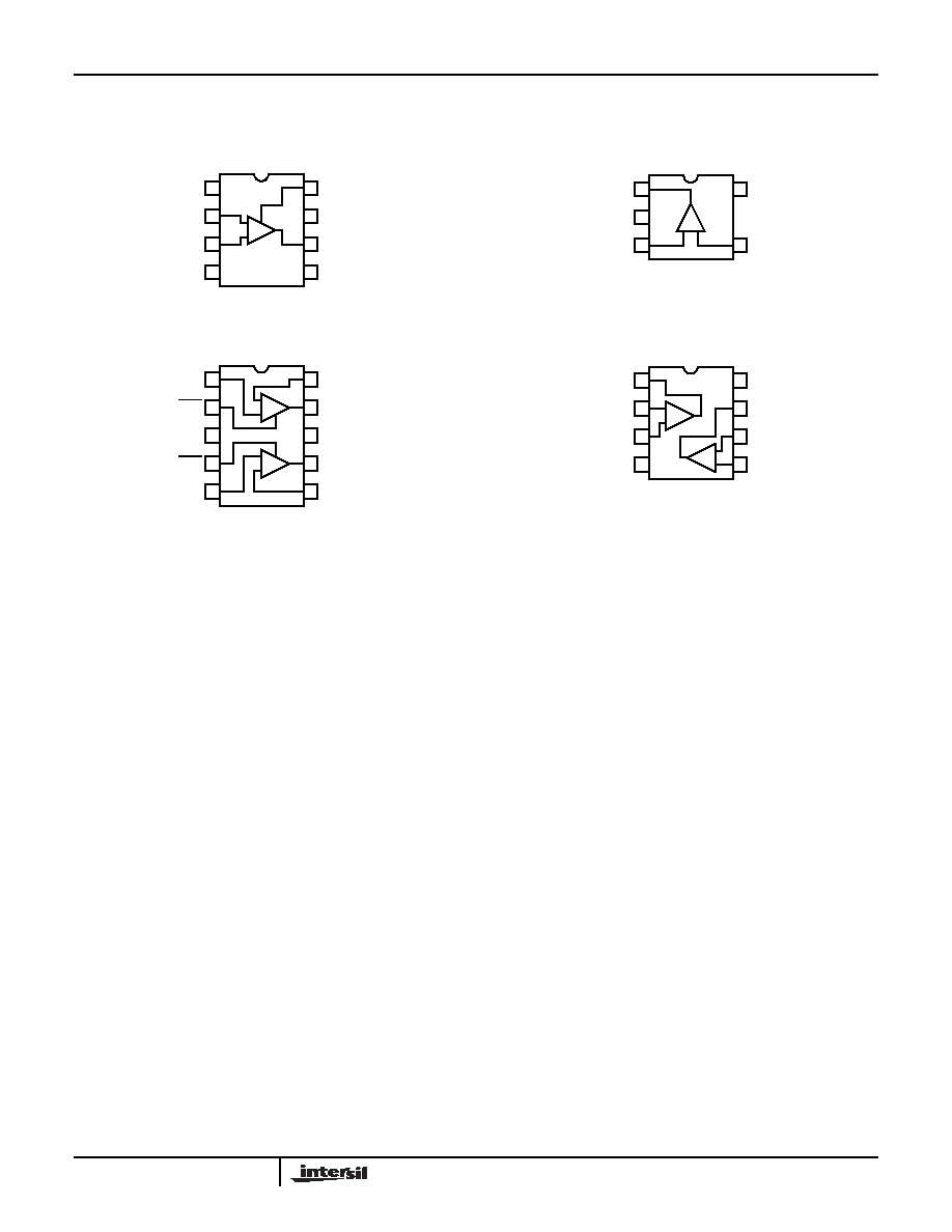
Pinouts
EL5134
(8 LD SO)
TOP VIEW
EL5135
(5 LD SOT-23)
TOP VIEW
EL5234
(10 LD MSOP)
TOP VIEW
EL5235
(8 LD SO)
TOP VIEW
1
2
3
4
8
7
6
5
-
+
NC
IN-
IN+
VS-
CE
VS+
OUT
NC
1
2
3
5
4
-
+
OUT
VS-
IN+
VS+
IN-
1
2
3
4
10
9
8
7
5
6
-
+
-
+
INA+
CEA
VS-
CEB
INA-
OUTA
VS+
OUTB
INB+
INB-
1
2
3
4
8
7
6
5
-
+
-
+
OUTA
INA-
INA+
VS-
VS+
OUTB
INB-
INB+
EL5134, EL5135, EL5234, EL5235
3
FN7383.2
October 3, 2005
Absolute Maximum Ratings
(T
A
= 25°C)
Supply Voltage from V
S
+ to V
S
- . . . . . . . . . . . . . . . . . . . . . . . 13.2V
SR, Supply Rate of Supply Voltage Slew. . . . . . . . . Maximum 1V/µs
I
IN
-, I
IN
+, CE . . . . . . . . . . . . . . . . . . . . . . . . . . . . . . . . . . . . . . ±5mA
Continuous Output Current . . . . . . . . . . . . . . . . . . . . . . . . . . 100mA
Power Dissipation . . . . . . . . . . . . . . . . . . . . . . . . . . . . . See Curves
Storage Temperature . . . . . . . . . . . . . . . . . . . . . . . .-65°C to +125°C
Operating Temperature . . . . . . . . . . . . . . . . . . . . . . .-40°C to +85°C
Operating Junction Temperature . . . . . . . . . . . . . . . . . . . . . . +125°C
CAUTION: Stresses above those listed in "Absolute Maximum Ratings" may cause permanent damage to the device. This is a stress only rating and operation of the
device at these or any other conditions above those indicated in the operational sections of this specification is not implied.
IMPORTANT NOTE: All parameters having Min/Max specifications are guaranteed. Typical values are for information purposes only. Unless otherwise noted, all tests
are at the specified temperature and are pulsed tests, therefore: T
J
= T
C
= T
A
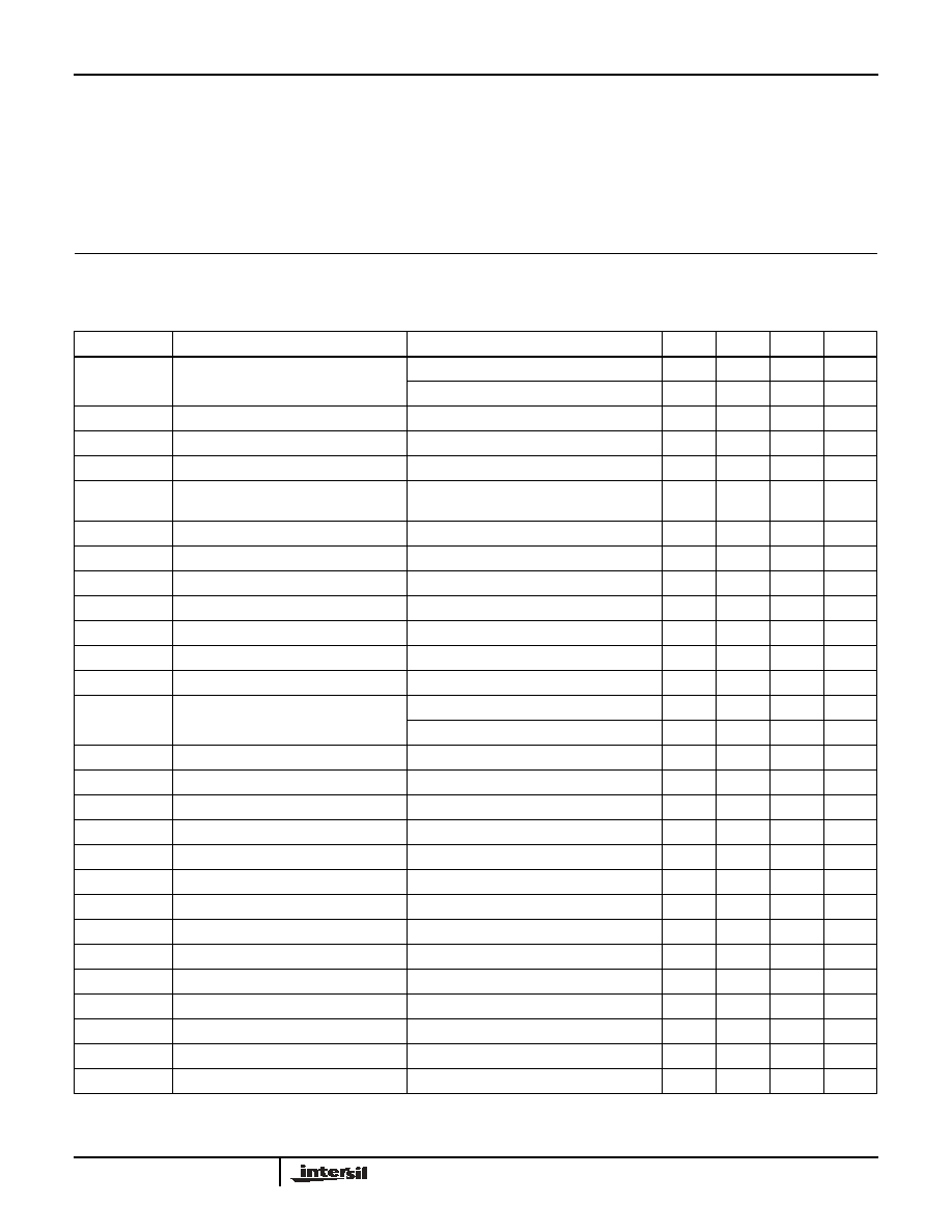
Electrical Specifications
V
S
+ = +5V, V
S
- = -5V, R
L
= 500
,
R
F
= 100
, R
G
= 25
,
T
A
= 25°C, unless otherwise specified
.
PARAMETER
DESCRIPTION
CONDITIONS
MIN
TYP
MAX
UNIT
V
OS
Offset Voltage
-1
0.2
1
mV
EL5234
0.3
±1.5
mV
T
C
V
OS
Offset Voltage Temperature Coefficient
Measured from T
MIN
to T
MAX
-0.8
µV/°C
IB
Input Bias Current
V
IN
= 0V
2.5
3.7
5.5
µA
I
OS
Input Offset Current
V
IN
= 0V
-0.7
0.3
0.7
nA
T
C
I
OS
Input Bias Current Temperature
Coefficient
Measured from T
MIN
to T
MAX
-3
nA/°C
PSRR
Power Supply Rejection Ratio
V
S
+ = 4.75V to 5.25V
75
85
dB
CMRR
Common Mode Rejection Ratio
V
CM
= ±3V
80
108
dB
CMIR
Common Mode Input Range
Guaranteed by CMRR test
±3
±3.3
V
R
IN
Input Resistance
Common mode
5
16
M
C
IN
Input Capacitance
1
pF
I
S
Supply Current
5.6
6.7
7.8
mA
AVOL
Open Loop Gain
R
L
= 1k
to GND
4.0
8.0
kV/V
V
O
Voltage Swing
R
L
= 1k
, R
F
= 900
, R
G
= 100
±3.5
3.9
V
R
L
= 150
, R
F
= 900
, R
G
= 100
±3.3
3.65
V
I
SC
Short Circuit Current
R
L
= 10
70
140
mA
BW
-3dB Bandwidth
A
V
= 5, R
L
= 1k
600
MHz
BW
±0.1dB Bandwidth
A
V
= 5, R
L
= 1k
40
MHz
GBWP
Gain Bandwidth Product
1500
MHz
PM
Phase Margin
R
L
= 1k
, C
L
= 6pF
55
°
SR
Slew Rate
V
S
= +5V, R
L
= 150
, V
OUT
= 0V to 3V
350
475
V/µs
t
R
Rise Time
±0.1V
STEP
1.75
ns
t
F
Fall Time
±0.1V
STEP
1.75
ns
OS
Overshoot
±0.1V
STEP
25
%
t
S
0.01% Settling Time
14
ns
dG
Differential Gain
A
V
= 5, R
F
= 1k
0.01
%
dP
Differential Phase
A
V
= 5, R
F
= 1k
0.01
°
e
N
Input Noise Voltage
f = 10kHz
1.9
nV/
Hz
i
N
Input Noise Current
f = 10kHz
0.9
pA/
Hz
EL5134, EL5135, EL5234, EL5235
4
FN7383.2
October 3, 2005
SUPPLY (EL5134, EL5234)
I
SOFF+
Supply Current - Disabled, per Amplifier
0
+25
µA
I
SOFF-
Supply Current - Disabled, per Amplifier
No load, V
IN
= 0V
-25
-14
0
µA
ENABLE (EL5134, EL5234)
I
IHCE
CE Pin Input High Current
CE = V
S
+
1
10
+25
µA
I
ILCE
CE Pin Input Low Current
CE = (V
S
+) -5V
-1
0
+1
µA
V
IHCE
CE Input High Voltage for Power-down
V
S
+ - 1
V
V
ILCE
CE Input Low Voltage for Power-down
V
S
+ - 3
V
Electrical Specifications
V
S
+ = +5V, V
S
- = -5V, R
L
= 500
,
R
F
= 100
, R
G
= 25
,
T
A
= 25°C, unless otherwise specified
. (Continued)
PARAMETER
DESCRIPTION
CONDITIONS
MIN
TYP
MAX
UNIT
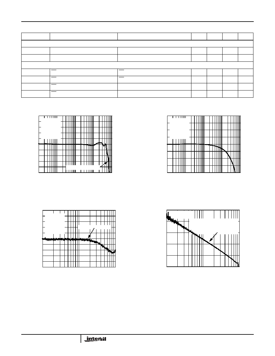
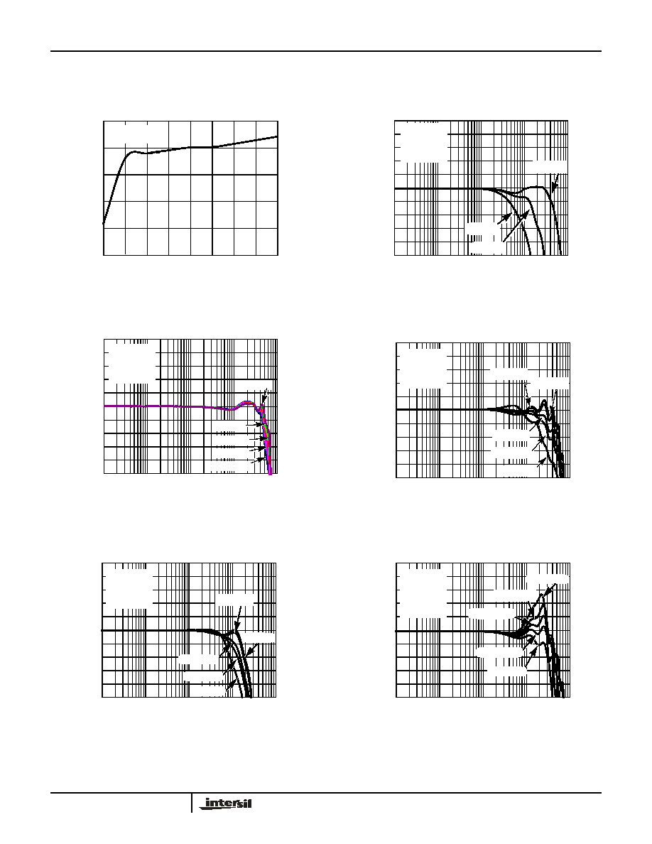
Typical Performance Curves
FIGURE 1. GAIN vs FREQUENCY (-3dB BANDWIDTH)
FIGURE 2. PHASE vs FREQUENCY
FIGURE 3. 0.1dB BANDWIDTH
FIGURE 4. GAIN BANDWIDTH PRODUCT
-5
-4
-3
-1
0
1
2
3
4
5
0.1
1
10
100
1K
FREQUENCY (MHz)
NORMALIZED GAIN
(
d
B)
-3dB BW @ 667MHz
-2
V
S
= ±5V
A
V
= +5
R
G
= 25
R
L
= 500
C
L
= 5pF
-240
-180
-60
60
120
180
240
0.1
1
10
100
1K
FREQUENCY (MHz)
PHASE
(
°
)
-120
V
S
= ±5V
A
V
= +5
R
G
= 25
R
L
= 500
C
L
= 5pF
0
1
10
100
FREQUENCY (MHz)
NORM
ALIZED GAIN
(dB)
-0.5
-0.4
-0.3
-0.2
-0.1
0
0.1
0.2
0.3
0.4
0.5
0.1dB BW @ 40MHz
V
S
= ±5V
A
V
= +5
R
G
= 25
R
L
= 500
C
L
= 5pF
GAIN = 40dB or 100
FREQUENCY = 15.9MHz
GAIN BW PRODUCT = 15.9 x 100
= 1590MHz
20
30
40
50
60
70
1
10
100
FREQUENCY (MHz)
GAIN (d
B)
V
S
= ±5V
R
L
= 500
EL5134, EL5135, EL5234, EL5235
5
FN7383.2
October 3, 2005
FIGURE 5. GAIN BANDWIDTH PRODUCT vs SUPPLY
VOLTAGES
FIGURE 6. GAIN vs FREQUENCY FOR VARIOUS +A
V
FIGURE 7. GAIN vs FREQUENCY FOR VARIOUS ±V
S
FIGURE 8. GAIN vs FREQUENCY FOR VARIOUS R
LOAD
(A
V
= +5)
FIGURE 9. GAIN vs FREQUENCY FOR VARIOUS R
LOAD
(A
V
= +10)
FIGURE 10. GAIN vs FREQUENCY FOR VARIOUS C
LOAD
(A
V
= +5)
Typical Performance Curves
(Continued)
800
1000
1200
1400
1600
1800
2.0
2.5
3.0
3.5
4.0
4.5
5.0
5.5
6.0
SUPPLY VOLTAGES (±V)
GA
IN BA
NDW
IDTH
P
R
ODUC
T (
M
H
z)
V
S
= ±5V
R
L
= 500
-5
-4
-3
-2
-1
0
1
2
3
4
5
0.1
1
10
100
1K
FREQUENCY (MHz)
NORMALIZE
D
GA
IN
(dB
)
A
V
= +20
A
V
= +5
A
V
= +10
V
S
= ±5V
R
G
= 25
R
L
= 500
C
L
= 5pF
A
V
= +20
A
V
= +10
-5
-4
-3
-2
-1
0
1
2
3
4
5
0.1
1K
FREQUENCY (MHz)
N
O
RMAL
IZED GAIN
(dB)
V
S
= ±6V
1
10
100
V
S
= ±3V
A
V
= +5V
R
G
= 25
R
L
= 500
C
L
= 5pF
V
S
= ±5V
V
S
= ±4V
V
S
= ±2.5V
-5
-4
-3
-2
-1
0
1
2
3
4
5
0.1
1K
FREQUENCY (MHz)
NORMAL
IZED GAIN
(dB)
1
10
100
V
S
= ±5V
A
V
= +5
R
L
= 500
C
L
= 5pF
R
L
= 1k
R
L
= 150
R
L
= 500
R
L
= 100
R
L
= 50
-5
-4
-3
-2
-1
0
1
2
3
4
5
0.1
1K
FREQUENCY (MHz)
NORMALIZED GAIN
(dB)
1
10
100
R
L
= 100
R
L
= 150
R
L
= 1k
R
L
= 500
R
L
= 50
V
S
= ±5V
A
V
= +10
R
G
= 25
C
L
= 10pF
-5
-4
-3
-2
-1
0
1
2
3
4
5
0.1
1K
FREQUENCY (MHz)
NORMALIZED GAIN
(dB)
1
10
100
C
L
= 18pF
C
L
= 12pF
C
L
= 8.2pF
C
L
= 4.7pF
C
L
= 0pF
V
S
= ±5V
A
V
= +5
R
G
= 25
R
F
= 100
R
L
= 500
EL5134, EL5135, EL5234, EL5235