1
Æ
FN7384.4
CAUTION: These devices are sensitive to electrostatic discharge; follow proper IC Handling Procedures.
1-888-INTERSIL or 321-724-7143
|
Intersil (and design) is a registered trademark of Intersil Americas Inc.
Copyright © Intersil Americas Inc. 2004-2005. All Rights Reserved.
All other trademarks mentioned are the property of their respective owners.
EL5150, EL5151, EL5250, EL5251, EL5451
200MHz Amplifiers
The EL5150, EL5151, EL5250, EL5251, and EL5451 are
200MHz bandwidth -3dB voltage mode feedback amplifiers
with DC accuracy of 0.01%, 1mV offsets and 10kV/V open
loop gains. These amplifiers are ideally suited for
applications ranging from precision measurement
instrumentation to high speed video and monitor
applications. Capable of operating with as little as 1.4mA of
current from a single supply ranging from 5V to 12V, dual
supplies ranging from ±2.5V to ±5.0V, these amplifiers are
also well suited for handheld, portable and battery-powered
equipment.
Single amplifiers are offered in SOT-23 packages and duals
in a 10-pin MSOP package for applications where board
space is critical. Quad amplifiers are available in a 14-pin SO
package. Additionally, singles and duals are available in the
industry-standard 8-pin SO package. All parts operate over
the industrial temperature range of -40∞C to +85∞C.
Features
∑ 200MHz -3dB bandwidth
∑ 67V/µs slew rate
∑ Very high open loop gains 50kV/V
∑ Low supply current = 1.4mA
∑ Single supplies from 5V to 12V
∑ Dual supplies from ±2.5V to ±5V
∑ Fast disable on the EL5150 and EL5250
∑ Low cost
∑ Pb-free available (RoHS compliant)
Applications
∑ Imaging
∑ Instrumentation
∑ Video
∑ Communications devices
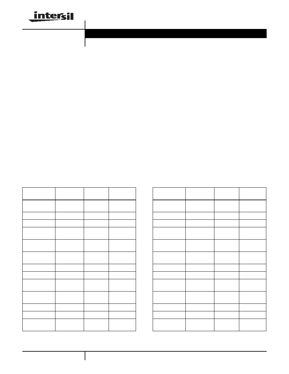
Ordering Information
PART NUMBER
PACKAGE
TAPE &
REEL
PKG. DWG. #
PART NUMBER
PACKAGE
TAPE &
REEL
PKG. DWG. #
EL5150IS
8-Pin SO
-
MDP0027
EL5151IWZ-T7A
(See Note)
5-Pin SOT-23
(Pb-Free)
7" (250 pcs)
MDP0038
EL5150IS-T7
8-Pin SO
7"
MDP0027
EL5250IY
10-Pin MSOP
-
MDP0043
EL5150IS-T13
8-Pin SO
13"
MDP0027
EL5250IY-T7
10-Pin MSOP
7"
MDP0043
EL5150ISZ
(See Note)
8-Pin SO
(Pb-Free)
-
MDP0027
EL5250IY-T13
10-Pin MSOP
13"
MDP0043
EL5150ISZ-T7
(See Note)
8-Pin SO
(Pb-Free)
7"
MDP0027
EL5251IS
8-Pin SO
-
MDP0027
EL5150ISZ-T13
(See Note)
8-Pin SO
(Pb-Free)
13"
MDP0027
EL5251IS-T7
8-Pin SO
7"
MDP0027
EL5150IW-T7
6-Pin SOT-23
7" (3K pcs)
MDP0038
EL5251IS-T13
8-Pin SO
13"
MDP0027
EL5150IW-T7A
6-Pin SOT-23
7" (250 pcs)
MDP0038
EL5251IY
8-Pin MSOP
-
MDP0043
EL5150IWZ-T7
(See Note)
6-Pin SOT-23
(Pb-Free)
7" (3K pcs)
MDP0038
EL5251IY-T7
8-Pin MSOP
7"
MDP0043
EL5150IWZ-T7A
(See Note)
6-Pin SOT-23
(Pb-Free)
7" (250 pcs)
MDP0038
EL5251IY-T13
8-Pin MSOP
13"
MDP0043
EL5151IW-T7
5-Pin SOT-23
7" (3K pcs)
MDP0038
EL5451IS
14-Pin SO
-
MDP0027
EL5151IW-T7A
5-Pin SOT-23
7" (250 pcs)
MDP0038
EL5451IS-T7
14-Pin SO
7"
MDP0027
EL5151IWZ-T7
(See Note)
5-Pin SOT-23
(Pb-Free)
7" (3K pcs)
MDP0038
EL5451IS-T13
14-Pin SO
13"
MDP0027
NOTE: Intersil Pb-free products employ special Pb-free material sets; molding compounds/die attach materials and 100% matte tin plate termination
finish, which are RoHS compliant and compatible with both SnPb and Pb-free soldering operations. Intersil Pb-free products are MSL classified at
Pb-free peak reflow temperatures that meet or exceed the Pb-free requirements of IPC/JEDEC J STD-020C.
Data Sheet
February 14, 2005
2
FN7384.4
February 14, 2005
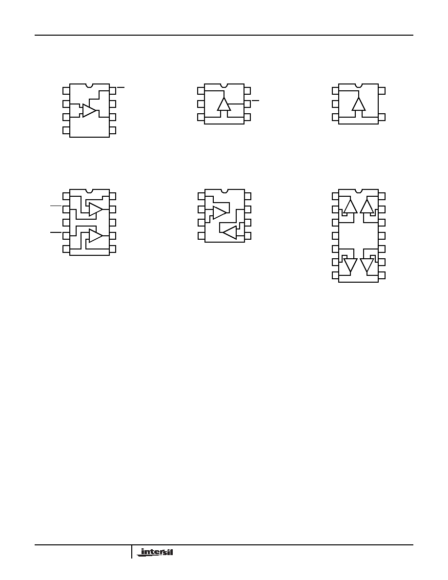
Pinouts
EL5150
(8-PIN SO)
TOP VIEW
EL5150
(6-PIN SOT-23)
TOP VIEW
EL5151
(5-PIN SOT-23)
TOP VIEW
EL5250
(10-PIN MSOP)
TOP VIEW
EL5251
(8-PIN MSOP)
TOP VIEW
EL5451
(14-PIN SO)
TOP VIEW
1
2
3
4
8
7
6
5
-
+
NC
IN-
IN+
VS-
CE
VS+
OUT
NC
1
2
3
6
4
5
-
+
OUT
VS-
IN+
VS+
IN-
CE
1
2
3
5
4
-
+
OUT
VS-
IN+
VS+
IN-
1
2
3
4
10
9
8
7
5
6
-
+
-
+
INA+
CEA
VS-
CEB
INA-
OUTA
VS+
OUTB
INB+
INB-
1
2
3
4
8
7
6
5
-
+
-
+
OUTA
INA-
INA+
VS-
VS+
OUTB
INB-
INB+
OUTA
INA-
INA+
VS+
OUTD
IND-
IND+
VS-
INB+
INC+
1
2
3
4
14
13
12
11
5
6
7
10
9
8
INC-
OUTC
INB-
OUTB
- +
-
+
- +
-
+
EL5150, EL5151, EL5250, EL5251, EL5451

3
FN7384.4
February 14, 2005
Absolute Maximum Ratings
(T
A
= 25∞C)
Supply Voltage between V
S
and GND. . . . . . . . . . . . . . . . . . . 13.2V
Maximum Continuous Output Current . . . . . . . . . . . . . . . . . . . 40mA
Pin Voltages . . . . . . . . . . . . . . . . . . . . . . . . . GND -0.5V to V
S
+0.5V
Power Dissipation . . . . . . . . . . . . . . . . . . . . . . . . . . . . . See Curves
Junction Temperature . . . . . . . . . . . . . . . . . . . . . . .-40∞C to +125∞C
Storage Temperature . . . . . . . . . . . . . . . . . . . . . . . .-65∞C to +150∞C
Ambient Operating Temperature . . . . . . . . . . . . . . . .-40∞C to +85∞C
Current into I
N
+, I
N
-, CE . . . . . . . . . . . . . . . . . . . . . . . . . . . . . . 5mA
CAUTION: Stresses above those listed in "Absolute Maximum Ratings" may cause permanent damage to the device. This is a stress only rating and operation of the
device at these or any other conditions above those indicated in the operational sections of this specification is not implied.
IMPORTANT NOTE: All parameters having Min/Max specifications are guaranteed. Typical values are for information purposes only. Unless otherwise noted, all tests
are at the specified temperature and are pulsed tests, therefore: T
J
= T
C
= T
A
Electrical Specifications
V
S
+ = +5V, V
S
- = -5V, R
L
= 150
, T
A
= 25∞C, unless otherwise specified.
PARAMETER
DESCRIPTION
CONDITIONS
MIN
TYP
MAX
UNIT
AC PERFORMANCE
BW
-3dB Bandwidth
A
V
= +1, R
L
= 500
200
MHz
A
V
= +2, R
L
= 150
40
MHz
GBWP
Gain Bandwidth Product
A
V
= 500
40
MHz
BW1
0.1dB Bandwidth
A
V
= +1, R
L
= 500
10
MHz
SR
Slew Rate
V
O
= ±2.5V, A
V
= +2
50
67
V/µs
V
O
= ±3.0V, A
V
= 1, R
L
= 500
100
V/µs
t
S
0.1% Settling Time
V
OUT
= -1V to +1V, A
V
= -2
80
ns
dG
Differential Gain Error (Note 1)
A
V
= +2, R
L
= 150
0.04
%
dP
Differential Phase Error (Note 1)
A
V
= +2, R
L
= 150
0.9
∞
V
N
Input Referred Voltage Noise
12
nV/
Hz
I
N
Input Referred Current Noise
1.0
pA/
Hz
DC PERFORMANCE
V
OS
Offset Voltage
-1
0.5
1
mV
T
C
V
OS
Input Offset Voltage Temperature
Coefficient
Measured from T
MIN
to T
MAX
-2
µV/∞C
A
VOL
Open Loop Gain
15
56
kV/V
INPUT CHARACTERISTICS
CMIR
Common Mode Input Range
Guaranteed by CMRR test
-3.5
+3.5
V
CMRR
Common Mode Rejection Ratio
85
100
dB
I
B
Input Bias Current
-100
20
+100
nA
I
OS
Input Offset Current
-30
6
30
nA
R
IN
Input Resistance
80
170
M
C
IN
Input Capacitance
1
pF
OUTPUT CHARACTERISTICS
V
OUT
Output Voltage Swing Low
R
L
= 150
to GND
±2.5
±2.8
V
R
L
= 500
to GND
±3.1
±3.4
V
I
OUT
Output Current
R
L
= 10
to GND
±40
±70
mA
EL5150, EL5151, EL5250, EL5251, EL5451

4
FN7384.4
February 14, 2005
ENABLE (SELECTED PACKAGES ONLY)
t
EN
Enable Time
EL5150
210
ns
t
DIS
Disable Time
EL5150
620
ns
I
IHCE
CE Pin Input High Current
CE = V
S
+
1
5
25
µA
I
ILCE
CE Pin Input Low Current
CE = V
S
+ - 5V
-1
0
+1
µA
V
IHCE
CE Input High Voltage for Powerdown
Disable
V
S
+ -1
V
V
ILCE
CE Input Low Voltage for Powerdown
Enable
V
S
+ -3
V
SUPPLY
I
SON
Supply Current - Enabled (per amplifier)
No load, V
IN
= 0V, CE = +5V
1.12
1.35
1.6
mA
I
SOFF+
Supply Current - Disabled (per amplifier)
-10
-1
+5
µA
I
SOFF-
Supply Current - Disabled (per amplifier) No load, V
IN
= 0V
-25
-14
0
µA
PSRR
Power Supply Rejection Ratio
DC, V
S
= ±3.0V to ±6.0V
80
110
dB
NOTE:
1. Standard NTSC test, AC signal amplitude = 286mV
P-P
, f = 3.58MHz, V
OUT
is swept from 0.8V to 3.4V, R
L
is DC coupled.
Electrical Specifications
V
S
+ = +5V, V
S
- = -5V, R
L
= 150
, T
A
= 25∞C, unless otherwise specified. (Continued)
PARAMETER
DESCRIPTION
CONDITIONS
MIN
TYP
MAX
UNIT
Typical Performance Curves
FIGURE 1. EL5150 FREQUENCY vs OPEN LOOP
GAIN/PHASE
FIGURE 2. PHASE vs FREQUENCY FOR VARIOUS GAINS
1K
1G
10K
100K
1M
10M
100M
100
80
60
40
20
0
180
135
0
-45
90
45
GAI
N
(d
B)
FREQUENCY (Hz)
P
HASE (∞)
100K
1G
1M
10M
100M
180
90
0
-90
-180
-270
P
HASE (∞)
FREQUENCY (Hz)
A
V
=+1
R
L
=500
R
F
=0
A
V
=+2
R
L
=150
R
F
=400
A
V
=+5
R
L
=500
R
F
=1.5K
EL5150, EL5151, EL5250, EL5251, EL5451

5
FN7384.4
February 14, 2005
FIGURE 3. EL5150 GAIN vs FREQUENCY FOR VARIOUS R
L
FIGURE 4. EL5150 GAIN vs FREQUENCY FOR VARIOUS R
L
FIGURE 5. EL5150 GAIN vs FREQUENCY FOR VARIOUS R
L
FIGURE 6. EL5150 GAIN vs FREQUENCY FOR VARIOUS C
L
FIGURE 7. EL5150 GAIN vs FREQUENCY FOR VARIOUS C
L
FIGURE 8. EL5150 GAIN vs FREQUENCY FOR VARIOUS C
L
Typical Performance Curves
(Continued)
100K
1G
1M
10M
100M
5
3
1
-1
-3
-5
NORMALIZED GAIN
(dB)
FREQUENCY (Hz)
A
V
=+1
C
L
=5pF
R
L
=100
R
L
=500
R
L
=300
R
L
=200
0.1
100
1
10
5
3
1
-1
-3
-5
NORMALIZED GAIN
(dB)
FREQUENCY (Hz)
V
S
=±5V
A
V
=+2
R
F
=R
G
=402
R
L
=1k
R
L
=100
R
L
=150
R
L
=500
100K
1M
10M
100M
4
2
0
-2
-4
-6
NORMALIZ
E
D
GAIN
(dB)
FREQUENCY (Hz)
A
V
=+5
R
F
=1.5k
C
L
=5pF
R
L
=500
R
L
=100
R
L
=200
R
L
=400
100K
1M
10M
100M
5
3
1
-1
-3
-5
NORMALIZ
E
D
GAIN
(dB)
FREQUENCY (Hz)
A
V
=+1
R
L
=500
300M
C
L
=15pF
C
L
=0pF
C
L
=3.9pF
C
L
=8.2pF
100K
100M
1M
10M
5
3
1
-1
-3
-5
N
O
RMAL
IZED GAIN
(dB)
FREQUENCY (Hz)
A
V
=+2
R
L
=500
R
F
=R
G
=400
C
L
=68pF
C
L
=0pF
C
L
=47pF
C
L
=22pF
100K
30M
1M
10M
5
3
1
-1
-3
-5
N
O
RMAL
IZED GAIN
(dB)
FREQUENCY (Hz)
A
V
=+5
R
F
=1.5k
R
L
=500
C
L
=82pF
C
L
=0pF
C
L
=15pF
C
L
=47pF
C
L
=68pF
EL5150, EL5151, EL5250, EL5251, EL5451