1
Æ
FN7365.3
CAUTION: These devices are sensitive to electrostatic discharge; follow proper IC Handling Procedures.
1-888-INTERSIL or 321-724-7143
|
Intersil (and design) is a registered trademark of Intersil Americas Inc.
Copyright © Intersil Americas Inc. 2003-2004. All Rights Reserved. Elantec is a registered trademark of Elantec Semiconductor, Inc.
All other trademarks mentioned are the property of their respective owners.
EL5166, EL5167
1.4GHz Current Feedback Amplifiers with
Enable
The EL5166 and EL5167 amplifiers are of the current
feedback variety and exhibit a very high bandwidth of
1.4GHz at A
V
= +1 and 800MHz at A
V
= +2. This makes
these amplifiers ideal for today's high speed video and
monitor applications, as well as a number of RF and IF
frequency designs.
With a supply current of just 8.5mA and the ability to run
from a single supply voltage from 5V to 12V, these amplifiers
offer very high performance for little power consumption.
The EL5166 also incorporates an enable and disable
function to reduce the supply current to 13µA typical per
amplifier. Allowing the CE pin to float or applying a low logic
level will enable the amplifier.
The EL5167 is offered in the 5-pin SOT-23 package and the
EL5166 is available in the 6-pin SOT-23 as well as the
industry-standard 8-pin SO packages. Both operate over the
industrial temperature range of -40∞C to +85∞C.
Features
∑ Gain-of-1 bandwidth = 1.4GHz/gain-of-2
bandwidth = 800MHz
∑ 6000V/µs slew rate
∑ Single and dual supply operation from 5V to 12V
∑ Low noise = 1.5nV/
Hz
∑ 8.5mA supply current
∑ Fast enable/disable (EL5166 only)
∑ 600MHz family - (EL5164 and EL5165)
∑ 400MHz family - (EL5162 and EL5163)
∑ 200MHz family - (EL5160 and EL5161)
∑ Pb-Free Available (RoHS Compliant)
Applications
∑ Video amplifiers
∑ Cable drivers
∑ RGB amplifiers
∑ Test equipment
∑ Instrumentation
∑ Current to voltage converters
Pinouts
Ordering Information
PART NUMBER
PACKAGE
TAPE &
REEL
PKG. DWG. #
EL5166IS
8-Pin SO
-
MDP0027
EL5166IS-T7
8-Pin SO
7"
MDP0027
EL5166IS-T13
8-Pin SO
13"
MDP0027
EL5166ISZ
(See Note)
8-Pin SO
(Pb-free)
-
MDP0027
EL5166ISZ-T7
(See Note)
8-Pin SO
(Pb-free)
7"
MDP0027
EL5166ISZ-T13
(See Note)
8-Pin SO
(Pb-free)
13"
MDP0027
EL5166IW-T7
6-Pin SOT-23
7"
MDP0038
EL5167IC-T7
5-Pin SC-70
7"
P5.049
EL5167IW-T7
5-Pin SOT-23
7"
MDP0038
EL5166IW-T7A
6-Pin SOT-23
7"
MDP0038
EL5167IC-T7A
5-Pin SC-70
7"
P5.049
EL5167IW-T7A
5-Pin SOT-23
7"
MDP0038
NOTE: Intersil Pb-free products employ special Pb-free material sets;
molding compounds/die attach materials and 100% matte tin plate
termination finish, which are RoHS compliant and compatible with
both SnPb and Pb-free soldering operations. Intersil Pb-free products
are MSL classified at Pb-free peak reflow temperatures that meet or
exceed the Pb-free requirements of IPC/JEDEC J STD-020C.
1
2
3
5
4
1
2
3
6
4
5
1
2
3
4
8
7
6
5
1
2
3
4
8
7
6
5
EL5167
(5-PIN SOT-23, SC-70)
TOP VIEW
-
+
OUT
VS-
IN+
VS+
IN-
-
+
OUT
VS-
IN+
VS+
IN-
CE
EL5166
(8-PIN SO)
TOP VIEW
-
+
NC
IN-
IN+
VS-
CE
VS+
OUT
NC
EL5166
(6-PIN SOT-23)
TOP VIEW
Data Sheet
December 13, 2004
2
FN7365.3
December 13, 2004
Absolute Maximum Ratings
(T
A
= 25∞C)
Supply Voltage between V
S
+ and V
S
- . . . . . . . . . . . . . . . . . . . 12.6V
Maximum Continuous Output Current . . . . . . . . . . . . . . . . . . . 50mA
I
OUT
. . . . . . . . . . . . . . . . . . . . . . . . . . . . . . . . . . . . . . . . . . . ±200mA
I into V
IN
+, V
IN
-, Enable Pins . . . . . . . . . . . . . . . . . . . . . . . . . ±4mA
Power Dissipation . . . . . . . . . . . . . . . . . . . . . . . . . . . . . See Curves
Pin Voltages. . . . . . . . . . . . . . . . . . . . . . . . . V
S
- -0.5V to V
S
+ +0.5V
Storage Temperature . . . . . . . . . . . . . . . . . . . . . . . .-65∞C to +150∞C
Ambient Operating Temperature . . . . . . . . . . . . . . . .-40∞C to +85∞C
Die Junction Temperature . . . . . . . . . . . . . . . . . . . . . . . . . . . . 125∞C
CAUTION: Stresses above those listed in "Absolute Maximum Ratings" may cause permanent damage to the device. This is a stress only rating and operation of the
device at these or any other conditions above those indicated in the operational sections of this specification is not implied.
IMPORTANT NOTE: All parameters having Min/Max specifications are guaranteed. Typical values are for information purposes only. Unless otherwise noted, all tests
are at the specified temperature and are pulsed tests, therefore: T
J
= T
C
= T
A
Electrical Specifications
V
S
+ = +5V, V
S
- = -5V, R
F
= 392
for A
V
= 1, R
F
= 250
for A
V
= 2, R
L
= 150
, T
A
= 25∞C
Unless Otherwise Specified.
PARAMETER
DESCRIPTION
CONDITIONS
MIN
TYP
MAX
UNIT
AC PERFORMANCE
BW
-3dB Bandwidth
A
V
= +1
1400
MHz
A
V
= +2
800
MHz
BW1
0.1dB Bandwidth
A
V
= +2
100
MHz
SR
Slew Rate
V
O
= -2.5V to +2.5V, A
V
= +2
4000
6000
V/µs
t
S
0.1% Settling Time
V
OUT
= -2.5V to +2.5V, A
V
= -1
8
ns
e
N
Input Voltage Noise
1.7
nV/
Hz
i
N
-
IN- Input Current Noise
19
pA/
Hz
i
N
+
IN+ Input Current Noise
50
pA/
Hz
dG
Differential Gain Error (Note 1)
A
V
= +2
0.01
%
dP
Differential Phase Error (Note 1)
A
V
= +2
0.03
∞
DC PERFORMANCE
V
OS
Offset Voltage
-5
-0.5
5
mV
T
C
V
OS
Input Offset Voltage Temperature
Coefficient
Measured from T
MIN
to T
MAX
3.52
µV/∞C
R
OL
Transimpedance
0.5
1.1
2.5
M
INPUT CHARACTERISTICS
CMIR
Common Mode Input Range
(guaranteed by CMRR test)
±3
±3.3
V
CMRR
Common Mode Rejection Ratio
52
57
66
dB
-ICMR
- Input Current Common Mode Rejection
-1
0.7
1
µA/V
+I
IN
+ Input Current
-25
0.7
25
µA
-I
IN
- Input Current
-25
8.5
25
µA
R
IN
Input Resistance
50
130
250
k
C
IN
Input Capacitance
1.5
pF
OUTPUT CHARACTERISTICS
V
O
Output Voltage Swing
R
L
= 150
to GND
±3.6
±3.8
±4.1
V
R
L
= 1k
to GND
±3.8
±4.0
±4.2
V
I
OUT
Output Current
R
L
= 10
to GND
±110
±160
±200
mA
EL5166, EL5167
3
FN7365.3
December 13, 2004
SUPPLY
I
SON
Supply Current - Enabled
No load, V
IN
= 0V
7.5
8.5
9.3
mA
I
SOFF+
Supply Current - Disabled
No load, V
IN
= 0V
1
4
25
µA
I
SOFF-
Supply Current - Disabled
No load, V
IN
= 0V
-25
-14
-1
µA
PSRR
Power Supply Rejection Ratio
DC, V
S
= ±4.75V to ±5.25V
70
50
dB
-IPSR
- Input Current Power Supply Rejection
DC, V
S
= ±4.75V to ±5.25V
-0.5
0.2
1
µA/V
ENABLE (EL5166 ONLY)
t
EN
Enable Time
170
ns
t
DIS
Disable Time
1.25
µs
I
IHCE
CE Pin Input High Current
CE = V
S
+
0
-1
µA
I
ILCE
CE Pin Input Low Current
CE = V
S
-
1
13
25
µA
V
IHCE
CE Input High Voltage for Power-down
V
S
+ -1
V
V
ILCE
CE Input Low Voltage for Power-down
V
S
+ -3
V
NOTE:
1. Standard NTSC test, AC signal amplitude = 286mV, f = 3.58MHz.
Electrical Specifications
V
S
+ = +5V, V
S
- = -5V, R
F
= 392
for A
V
= 1, R
F
= 250
for A
V
= 2, R
L
= 150
, T
A
= 25∞C
Unless Otherwise Specified. (Continued)
PARAMETER
DESCRIPTION
CONDITIONS
MIN
TYP
MAX
UNIT
EL5166, EL5167

4
FN7365.3
December 13, 2004
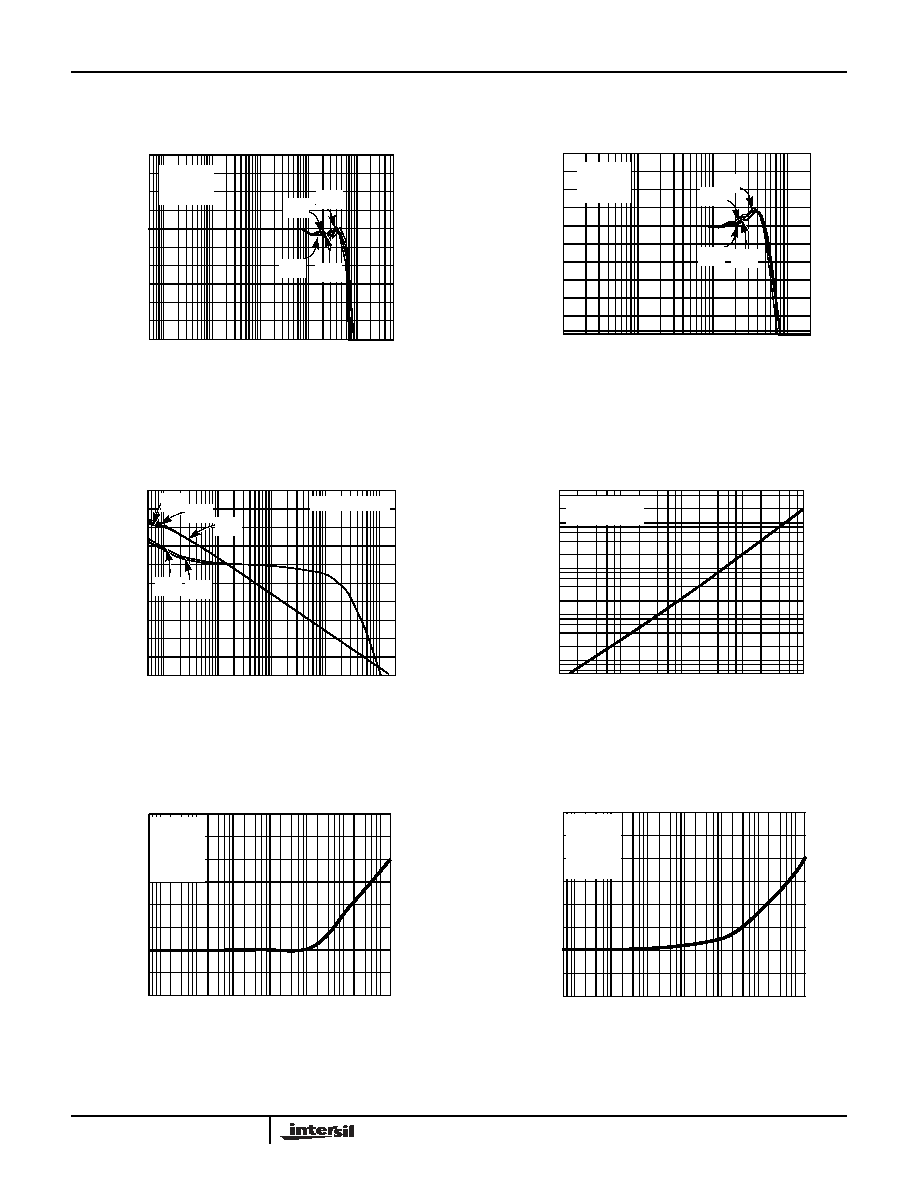
Typical Performance Curves
FIGURE 1. FREQUENCY RESPONSE AS THE FUNCTION OF
R
F
FIGURE 2. FREQUENCY RESPONSE AS THE FUNCTION OF
THE GAIN
FIGURE 3. FREQENCY RESPONSE vs C
IN
FIGURE 4. NON-INVERTING FREQUENCY RESPONSE FOR
VARIOUS C
IN
- (6-PIN SOT-23)
FIGURE 5. INVERTING FREQUENCY RESPONSE FOR GAIN
OF 1 AND 2
FIGURE 6. RISE AND FALL TIME (6-PIN SOT-23)
0
3
4
5
-5
-4
-3
-2
-1
1
2
NORMAL
IZED MAGNIT
UDE (dB)
R
F
=368
100K
10M
100M
1G
FREQUENCY (Hz)
1M
R
F
=392
R
F
=662
R
F
=511
R
F
=608
R
F
=698
R
F
=806
R
F
=900
R
F
=1K
V
CC
=5V
V
EE
=-5V
R
L
=150
100K
10M
100M
1G
FREQUENCY (Hz)
1M
4
3
2
1
0
-3
-5
-1
-2
-4
NORMALIZE
D
MAGNITUDE (
d
B
)
-6
R
G
=43
R
G
=392
R
G
=186
R
G
=93
V
CC
=5V
V
EE
=-5V
R
L
=150
R
F
=392
C=0p
5
4
3
2
1
-2
-4
0
-1
-3
NORMALIZE
D
MAGNITUDE (
d
B
)
-5
100K
1M
10M
100M
1G
FREQUENCY (Hz)
C=1p
C=1.5p
C=2.5p
C=4.7p
NOR
M
ALIZED GAIN
(dB)
100K
10M
100M
1G
FREQUENCY (Hz)
1M
C=4.7p
C=2.5p
C=0
C=1.5p
V
CC
=+V
V
EE
=-5V
RL=150W
V
CC
=+5V
V
EE
=-5V
R
L
=150
R
F
=R
G
=392
C=1p
NORMALIZ
E
D
GA
IN
(dB)
1M
100M
1G
FREQUENCY (Hz)
10M
R
F
=220
R
G
=220
R
F
=220
R
G
=100
V
CC
, V
EE
=5V
0.
5
V
/
D
IV
2ns/DIV
EL5166, EL5167
5
FN7365.3
December 13, 2004
FIGURE 7. FREQUENCY RESPONSE AS THE FUNCTION OF
THE POWER SUPPLY VOLTAGE
FIGURE 8. INVERTING AMPLIFIER, FREQUENCY
RESPONSE AS THE FUNCTION OF V
CC
, V
EE
GAIN - 1
FIGURE 9. TRANSIMPEDANCE MAGNITUDE AND PHASE AS
THE FUNCTION OF THE FREQUENCY
FIGURE 10. CLOSED LOOP OUTPUT IMPEDANCE vs
FREQUENCY (6-PIN SOT-23)
FIGURE 11. PSRR +5V
FIGURE 12. PSRR -5V
Typical Performance Curves
(Continued)
NORMALIZED GAIN
(dB)
100K
1M
10M
100M
1G
FREQUENCY (Hz)
R
L
=150
R
F
=300
R
G
=300
6.0V
5.0V
2.5V
3.0V
1M
100M
1K
FREQUENCY (Hz)
10M
NORMALIZED GAIN
(dB)
R
L
=150
R
F
=220
R
G
=220
2.5V
3.5V
6.0V
5.0V
90
270
180
0
PH
A
S
E
(
∞
)
100K
10M
100M
1G
FREQUENCY (Hz)
1M
V
CC
, V
EE
=2.5V
10K
100
1K
100K
5.0V
2.5V
6.0V
5.0V
2.5V
10
10m
100m
1
10K
1M
10M
FREQUENCY (Hz)
100K
100M
V
CC
, V
EE
=5V
GAIN=2
0
10
20
30
40
50
60
70
P
S
RR (V
CC
) (
d
B)
80
100
10K
1M
10M
100M
FREQUENCY (Hz)
1K
100K
V
CC
=5V
V
EE
=-5V
R
L
=150
R
F
=402
R
G
=402
0
10
20
30
40
70
50
60
PSRR (V
EE
) (
d
B)
80
100
10K
1M
10M
100M
FREQUENCY (Hz)
1K
100K
V
CC
=5V
V
EE
=-5V
R
L
=150
R
F
=402
R
G
=402
EL5166, EL5167