Äîêóìåíòàöèÿ è îïèñàíèÿ www.docs.chipfind.ru
1
®
FN7309.5
EL5170, EL5370
100MHz Differential Twisted-Pair Drivers
The EL5170 and EL5370 are single and triple high
bandwidth amplifiers with a fixed gain of 2. They are
primarily targeted for applications such as driving twisted-
pair lines in component video applications. The inputs signal
can be in either single-ended or differential form but the
outputs are always in differential form.
The output common mode level for each channel is set by
the associated V
REF
pin, which have a -3dB bandwidth of
over 70MHz. Generally, these pins are grounded but can be
tied to any voltage reference.
All outputs are short circuit protected to withstand temporary
overload condition.
The EL5170 and EL5370 are specified for operation over the
full -40°C to +85°C temperature range.
Features
· Fully differential inputs and outputs
· Differential input range ±2.3V typ.
· 100MHz 3dB bandwidth at fixed gain of 2
· 1200V/µs slew rate
· Single 5V or dual ±5V supplies
· 50mA maximum output current
· Low power - 7.4mA per channel
· Pb-Free Available (RoHS Compliant)
Applications
· Twisted-pair drivers
· Differential line drivers
· VGA over twisted-pairs
· ADSL/HDSL drivers
· Single ended to differential amplification
· Transmission of analog signals in a noisy environment
Ordering Information
PART
NUMBER
PACKAGE
TAPE & REEL
PKG. DWG. #
EL5170IS
8-Pin SO
-
MDP0027
EL5170IS-T7
8-Pin SO
7"
MDP0027
EL5170IS-T13
8-Pin SO
13"
MDP0027
EL5170ISZ
(See Note)
8-Pin SO
(Pb-free)
-
MDP0027
EL5170ISZ-T7
(See Note)
8-Pin SO
(Pb-free)
7"
MDP0027
EL5170ISZ-
T13 (See Note)
8-Pin SO
(Pb-free)
13"
MDP0027
EL5170IY
8-Pin MSOP
-
MDP0043
EL5170IY-T7
8-Pin MSOP
7"
MDP0043
EL5170IY-T13
8-Pin MSOP
13"
MDP0043
EL5170IYZ
(See Note)
8-Pin MSOP
(Pb-free)
-
MDP0043
EL5170IYZ-T7
(See Note)
8-Pin MSOP
(Pb-free)
7"
MDP0043
EL5170IYZ-
T13 (See Note)
8-Pin MSOP
(Pb-free)
13"
MDP0043
EL5370IU
24-Pin QSOP
-
MDP0040
EL5370IU-T7
24-Pin QSOP
7"
MDP0040
EL5370IU-T13
24-Pin QSOP
13"
MDP0040
NOTE: Intersil Pb-free products employ special Pb-free material sets;
molding compounds/die attach materials and 100% matte tin plate
termination finish, which are RoHS compliant and compatible with
both SnPb and Pb-free soldering operations. Intersil Pb-free products
are MSL classified at Pb-free peak reflow temperatures that meet or
exceed the Pb-free requirements of IPC/JEDEC J STD-020C.
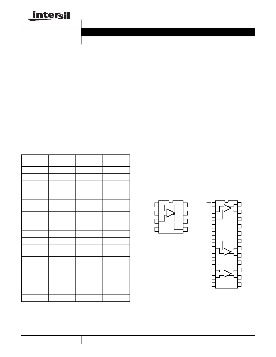
Pinouts
EL5170
(8-PIN SO, MSOP)
TOP VIEW
EL5370
(24-PIN QSOP)
TOP VIEW
1
2
3
4
8
7
6
5
-
+
IN+
EN
IN-
REF
OUT+
VS-
VS+
OUT-
1
2
3
4
16
15
14
13
5
6
7
12
11
9
8
10
20
19
18
17
24
23
22
21
-
+
EN
INP1
INN1
REF1
NC
INP2
INN2
REF2
NC
INP3
INN3
REF3
OUT1
OUT1B
NC
VSP
VSN
NC
OUT2
OUT2B
NC
OUT3
OUT3B
NC
-
+
-
+
Data Sheet
October 29, 2004
CAUTION: These devices are sensitive to electrostatic discharge; follow proper IC Handling Procedures.
1-888-INTERSIL or 321-724-7143
|
Intersil (and design) is a registered trademark of Intersil Americas Inc.
Copyright © Intersil Americas Inc. 2002-2004. All Rights Reserved.
All other trademarks mentioned are the property of their respective owners
.
2
FN7309.5
IMPORTANT NOTE: All parameters having Min/Max specifications are guaranteed. Typ values are for information purposes only. Unless otherwise noted, all tests are
at the specified temperature and are pulsed tests, therefore: T
J
= T
C
= T
A
Absolute Maximum Ratings
(T
A
= 25°C)
Supply Voltage (V
S
+ to V
S
-) . . . . . . . . . . . . . . . . . . . . . . . . . . 12.6V
Maximum Output Current. . . . . . . . . . . . . . . . . . . . . . . . . . . . ±60mA
Storage Temperature Range . . . . . . . . . . . . . . . . . .-65°C to +150°C
Operating Junction Temperature . . . . . . . . . . . . . . . . . . . . . . +135°C
Recommended Operating Temperature . . . . . . . . . .-40°C to +85°C
CAUTION: Stresses above those listed in "Absolute Maximum Ratings" may cause permanent damage to the device. This is a stress only rating and operation of the
device at these or any other conditions above those indicated in the operational sections of this specification is not implied.
Electrical Specifications
V
S
+ = +5V, V
S
- = -5V, T
A
= 25°C, V
IN
= 0V, A
V
= 2, R
LD
= 200
, C
LD
= 1pF, unless otherwise specified.
PARAMETER
DESCRIPTION
CONDITIONS
MIN
TYP
MAX
UNIT
AC PERFORMANCE
BW
-3dB Bandwidth
100
MHz
BW
± 0.1dB Bandwidth
12
MHz
SR
Slew Rate
V
OUT
= 2V
P-P
, 20% to 80%
800
1100
V/µs
T
STL
Settling Time to 0.1%
V
OUT
= 2V
P-P
20
ns
T
OVR
Output Overdrive Recovery time
40
ns
V
REF
BW
(-3dB) V
REF
-3dB Bandwidth
A
V
=1,
C
LD
= 2.7pF
70
MHz
V
REF
SR+
V
REF
Slew Rate - Rise
V
OUT
= 2V
P-P
, 20% to 80%
125
V/µs
V
REF
SR-
V
REF
Slew Rate - Fall
V
OUT
= 2V
P-P
, 20% to 80%
65
V/µs
V
N
Input Voltage Noise
f = 10kHz
28
nV/
Hz
HD2
Second Harmonic Distortion
V
OUT
= 2V
P-P
, 1MHz
-79
dBc
HD2
Second Harmonic Distortion
V
OUT
= 2V
P-P
, 10MHz
-65
dBc
HD3
Third Harmonic Distortion
V
OUT
= 2V
P-P
, 1MHz
-62
dBc
HD3
Third Harmonic Distortion
V
OUT
= 2V
P-P
, 10MHz
-43
dBc
dG
Differential Gain at 3.58MHz
R
LD
= 300
,
A
V
= 2
0.14
%
d
Differential Phase at 3.58MHz
R
LD
= 300
,
A
V
= 2
0.38
°
e
S
Channel Separation - For EL5370 only
at f = 1MHz
85
dB
INPUT CHARACTERISTICS
V
OS
Input Referred Offset Voltage
±6
±25
mV
I
IN
Input Bias Current (V
IN
, V
INB
)
-10
-6
-2
µA
I
REF
Input Bias Current at REF Pin
V
REF
= +3.2V
0.5
1.25
3
µA
V
REF
= -3.2V
-1
0
+1
µA
Gain
Gain Accuracy
V
IN
= ±1V
1.98
2
2.02
V
R
IN
Differential Input Resistance
300
k
C
IN
Differential Input Capacitance
1
pF
DMIR
Differential Mode Input Range
±2.1
±2.3
V
CMIR+
Common Mode Positive Input Range at
V
IN
+, V
IN
-
3.2
3.4
V
CMIR-
Common Mode Negative Input Range at
V
IN
+, V
IN
-
-4.5
-4.2
V
V
REFIN
Reference Input Voltage Range - Positive V
IN
+ = V
IN
- = 0V
3.4
3.8
V
Reference Input Voltage Range -
Negative
-3.3
-3
V
EL5170, EL5370
3
FN7309.5
V
REFOS
Output Offset Relative to V
REF
-140
60
+140
mV
CMRR
Input Common Mode Rejection Ratio
V
IN
= ±2.5V
65
84
dB
OUTPUT CHARACTERISTICS
V
OUT
Positive Output Voltage Swing
R
LD
= 200
3.3
3.6
V
Negative Output Voltage Swing
-3.3
-3
V
I
OUT
(Max)
Maximum Output Current
R
L
= 10
(EL5170)
±50
±80
mA
R
L
= 10
(EL5370)
±70
±85
mA
R
OUT
Output Impedance
60
m
SUPPLY
V
SUPPLY
Supply Operating Range
V
S
+ to V
S
-
4.75
11
V
I
S(ON)
Power Supply Current - Per channel
6
7.4
8.4
mA
I
S(OFF)
+
Positive Power Supply Current - Disabled EN pin tied to 4.8V (EL5170)
60
80
100
µA
I
S(OFF)
-
Negative Power Supply Current -
Disabled
-150
-120
-90
µA
I
S(OFF)
+
Positive Power Supply Current - Disabled EN pin tied to 4.8V (EL5370)
0.5
2
5
µA
I
S(OFF)
-
Negative Power Supply Current -
Disabled
-150
-120
-90
µA
PSRR
Power Supply Rejection Ratio
V
S
from ±4.5V to ±5.5V (EL5170)
70
83
dB
V
S
from ±4.5V to ±5.5V (EL5370)
65
83
dB
ENABLE
t
EN
Enable Time
200
ns
t
DS
Disable Time
1
µs
V
IH
EN Pin Voltage for Power-up
V
S
+ -
1.5
V
V
IL
EN Pin Voltage for Shut-down
V
S
+ -
0.5
V
I
IH-EN
EN Pin Input Current High - per channel
At V
EN
= 5V
40
50
µA
I
IL-EN
EN Pin Input Current Low - per channel
At V
EN
= 0V
-6
-3
µA
Electrical Specifications
V
S
+ = +5V, V
S
- = -5V, T
A
= 25°C, V
IN
= 0V, A
V
= 2, R
LD
= 200
, C
LD
= 1pF, unless otherwise specified.
PARAMETER
DESCRIPTION
CONDITIONS
MIN
TYP
MAX
UNIT
Pin Descriptions
EL5170
EL5370
PIN NAME
PIN FUNCTION
1
2, 6, 10
IN+, INP1, 2, 3
Non-inverting inputs
2
1
EN
Enable
3
3, 7, 11
IN-, INN1, 2, 3
Inverting inputs
4
4, 8, 12
REF1, 2, 3
Reference input, sets common-mode output voltage
5
14, 17, 23
OUT-, OUT1B, 2B, 3B Inverting outputs
6
21
VS+, VSP
Positive supply
7
20
VS-, VSN
Negative supply
8
15, 18, 24
OUT+, OUT1, 2, 3
Non-inverting outputs
5, 9, 13, 16, 19, 22
NC
No connects, grounded for best crosstalk performance
EL5170, EL5370
4
FN7309
.5
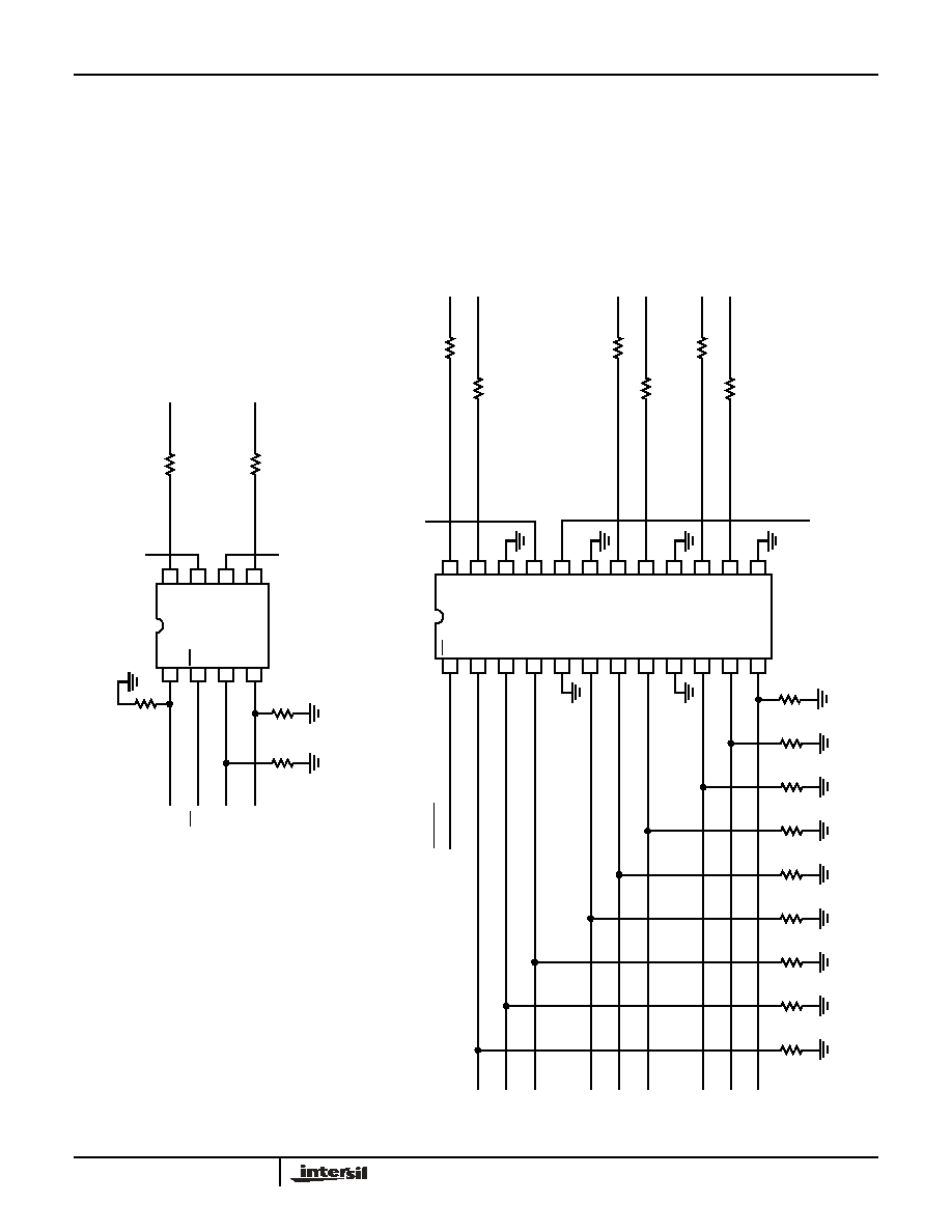
Connection Diagrams
INP
EN
INN
REF
OUT
VSN
VSP
OUTB
1
2
3
4
8
7
6
5
INP
EN
INN
REF
R
S1
50
R
S2
50
R
S3
50
50
LOADN
R
RT2
LOADP
-5V
+5V
EL5170
R
RT2
50
EL5370
1
2
3
4
16
15
14
13
5
6
7
12
11
9
8
10
20
19
18
17
24
23
22
21
EN
INP1
INN1
REF1
NC
INP2
INN2
REF2
NC
INP3
INN3
REF3
OUT1
OUT1B
NC
VSP
VSN
NC
OUT2
OUT2B
NC
OUT3
OUT3B
NC
R
SR3
50
R
SN3
50
R
SP3
50
R
SR2
50
R
SN2
50
R
SP2
50
R
SR1
50
R
SN1
50
R
SP1
50
INP1
INN1
REF1
INP2
INN2
REF2
INP3
INN3
REF3
ENABLE
-5V
+5V
50
R
RT3B
LD3B
50
R
RT3
LD3
50
R
RT2B
LD2B
50
R
RT2
LD2
50
R
RT1B
LD1B
50
R
RT1
LD1
EL5170, EL5370
5
FN7309.5
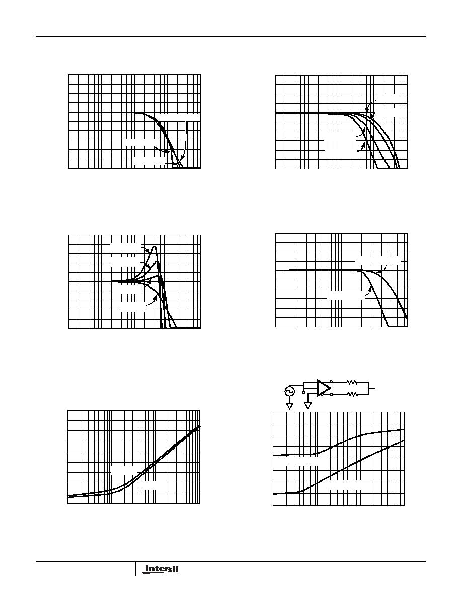
Typical Performance Curves
FIGURE 1. FREQUENCY RESPONSE
FIGURE 2. SMALL SIGNAL FREQUENCY RESPONSE vs R
LD
FIGURE 3. SMALL SIGNAL FREQUENCY RESPONSE vs C
LD
FIGURE 4. FREQUENCY RESPONSE vs V
REF
FIGURE 5. POWER SUPPLY REJECTION RATIO vs
FREQUENCY
FIGURE 6. COMMON MODE REJECTION vs FREQUENCY
100K
FREQUENCY (Hz)
10M
100M
1G
GAIN (d
B)
6
5
4
3
2
1
0
7
8
9
10
V
S
= ±5V, A
V
= 2, R
LD
= 200
, C
LD
= 1pF
V
OP-P
= 2V
V
OP-P
= 1V
V
OP-P
= 200mV
1M
1M
100M
1G
FREQUENCY (Hz)
100K
GAI
N
(
d
B)
6
5
4
3
2
1
0
7
8
9
10
C
LD
= 1pF, V
ODP-P
= 200mV
10M
R
LD
= 1k
R
LD
= 100
R
LD
= 500
R
LD
= 200
100K
FREQUENCY (Hz)
10M
100M
1G
GAI
N
(
d
B)
7
6
5
4
3
2
1
8
9
10
11
V
S
=
±5V
, R
LD
= 200
, V
ODP-P
= 200mV
C
LD
= 0pF
C
LD
= 20pF
C
LD
= 40pF
C
LD
= 75pF
1M
100M
FREQUENCY (Hz)
1M
GAIN (d
B)
0
-1
-2
-3
-4
-5
-6
1
2
3
4
10M
V
REF
= 200mV
P-P
V
REF
= 1V
P-P
0
-10
-30
-50
-60
-80
-90
1M
10M
100M
PS
RR (dB)
FREQUENCY (Hz)
-70
-40
-20
100K
PSRR-
PSRR+
100K
1M
10M
100M
FREQUENCY (Hz)
COMMON MODE REJE
C
T
ION (dB)
-10
-30
-50
-60
-80
-90
-70
-40
-20
-
+
V
OCM
V
ODM
100
100
V
OCM
/V
INCM
V
ODM
/V
INCM
V
INCM
EL5170, EL5370