Äîêóìåíòàöèÿ è îïèñàíèÿ www.docs.chipfind.ru
1
®
FN7491.1
EL5178, EL5378
700MHz Differential Twisted-Pair Drivers
The EL5178 and EL5378 are single and triple high
bandwidth amplifiers with an output in differential form. They
are primarily targeted for applications such as driving
twisted-pair lines in component video applications. The
inputs can be in either single-ended or differential form but
the outputs are always in differential form.
On the EL5178 and EL5378, two feedback inputs provide
the user with the ability to set the gain of each device (stable
at minimum gain of 2).
The output common mode level for each channel is set by
the associated REF pin, which have a -3dB bandwidth of
over 110MHz. Generally, these pins are grounded but can be
tied to any voltage reference.
All outputs are short circuit protected to withstand temporary
overload condition.
The EL5178 is available in 8-pin MSOP and SO packages
and EL5378 is available in a 28-pin QSOP package. All
specified for operation over the full -40°C to +85°C
temperature range.
Features
· Fully differential inputs, outputs, and feedback
· Differential input range ±2.3V
· 700MHz 3dB bandwidth
· 1000V/µs slew rate
· Low distortion at 5MHz and 20MHz
· Single 5V or dual ±5V supplies
· 60mA maximum output current
· Low power - 12.5mA per channel
· Pb-free available (RoHS compliant)
Applications
· Twisted-pair driver
· Differential line driver
· VGA over twisted-pair
· ADSL/HDSL driver
· Single ended to differential amplification
· Transmission of analog signals in a noisy environment
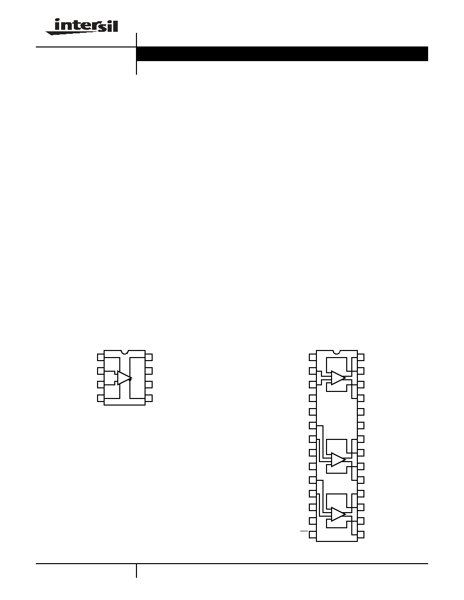
Pinouts
EL5178
(8-PIN MSOP, SO)
TOP VIEW
EL5378
(28-PIN QSOP)
TOP VIEW
-
+
FBP
IN+
REF
FBN
OUT+
VS-
VS+
OUT-
1
2
3
4
8
7
6
5
1
2
3
4
28
27
26
25
5
6
7
24
23
22
8
21
9
10
20
19
11
12
13
18
17
16
14
15
-
+
-
+
-
+
OUT1
FBP1
FBN1
OUT1B
VSP
VSN
OUT2
FBP2
FBN2
OUT2B
OUT3
FBP3
FBN3
OUT3B
NC
INP1
INN1
REF1
NC
INP2
INN2
REF2
NC
INP3
INN3
REF3
NC
EN
Data Sheet
March 8, 2005
CAUTION: These devices are sensitive to electrostatic discharge; follow proper IC Handling Procedures.
1-888-INTERSIL or 1-888-352-6832
|
Intersil (and design) is a registered trademark of Intersil Americas Inc.
Copyright Intersil Americas Inc. 2004, 2005. All Rights Reserved
All other trademarks mentioned are the property of their respective owners.
2
FN7491.1
March 8, 2005
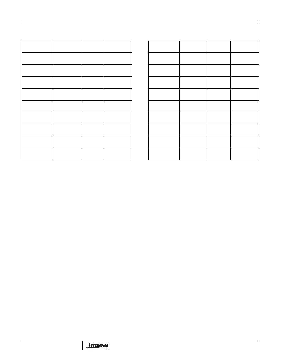
Ordering Information
PART
NUMBER
PACKAGE
TAPE &
REEL
PKG. DWG. #
PART
NUMBER
PACKAGE
TAPE &
REEL
PKG. DWG. #
EL5178IS
8-Pin SO
-
MDP0027
EL5178IYZ
(See Note)
8-Pin MSOP
(Pb-Free)
-
MDP0043
EL5178IS-T7
8-Pin SO
7"
MDP0027
EL5178IYZ-T7
(See Note)
8-Pin MSOP
(Pb-Free)
7"
MDP0043
EL5178IS-T13
8-Pin SO
13"
MDP0027
EL5178IYZ-T13
(See Note)
8-Pin MSOP
(Pb-Free)
13"
MDP0043
EL5178ISZ
(See Note)
8-Pin SO
(Pb-Free)
-
MDP0027
EL5378IU
28-Pin QSOP
-
MDP0040
EL5178ISZ-T7
(See Note)
8-Pin SO
(Pb-Free)
7"
MDP0027
EL5378IU-T7
28-Pin QSOP
7"
MDP0040
EL5178ISZ-T13
(See Note)
8-Pin SO
(Pb-Free)
13"
MDP0027
EL5378IU-T13
28-Pin QSOP
13"
MDP0040
EL5178IY
8-Pin MSOP
-
MDP0043
EL5378IUZ
(See Note)
28-Pin QSOP
(Pb-Free)
-
MDP0040
EL5178IY-T7
8-Pin MSOP
7"
MDP0043
EL5378IUZ-T7
(See Note)
28-Pin QSOP
(Pb-Free)
7"
MDP0040
EL5178IY-T13
8-Pin MSOP
13"
MDP0043
EL5378IUZ-T13
(See Note)
28-Pin QSOP
(Pb-Free)
13"
MDP0040
NOTE: Intersil Pb-free products employ special Pb-free material sets; molding compounds/die attach materials and 100% matte tin plate termination
finish, which are RoHS compliant and compatible with both SnPb and Pb-free soldering operations. Intersil Pb-free products are MSL classified at
Pb-free peak reflow temperatures that meet or exceed the Pb-free requirements of IPC/JEDEC J STD-020.
EL5178, EL5378
3
FN7491.1
March 8, 2005
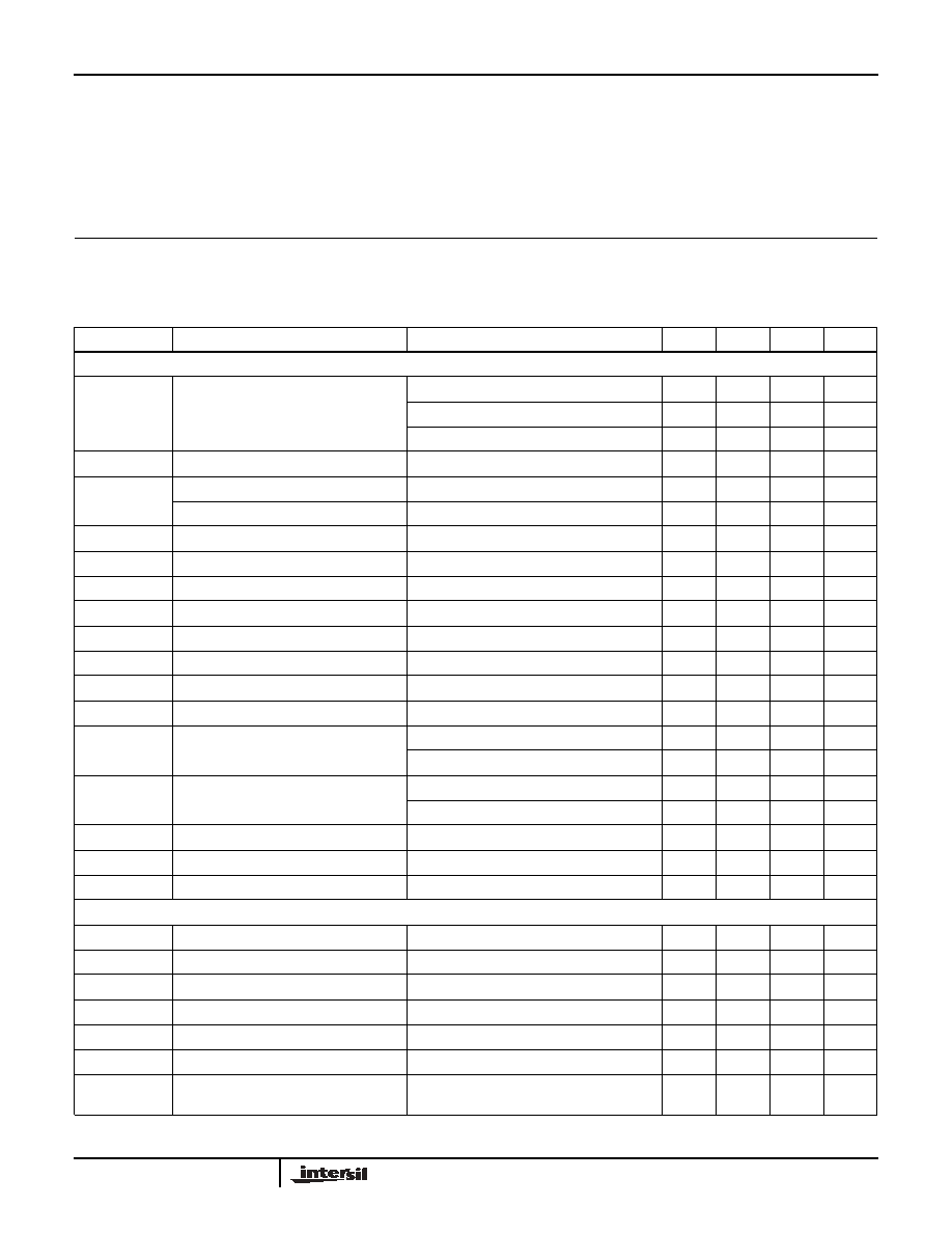
IMPORTANT NOTE: All parameters having Min/Max specifications are guaranteed. Typ values are for information purposes only. Unless otherwise noted, all tests are
at the specified temperature and are pulsed tests, therefore: T
J
= T
C
= T
A
Absolute Maximum Ratings
(T
A
= 25°C)
Supply Voltage (V
S
+ to V
S
-) . . . . . . . . . . . . . . . . . . . . . . . . . . . .12V
Maximum Output Current. . . . . . . . . . . . . . . . . . . . . . . . . . . . ±60mA
Input Current (all inputs and references) . . . . . . . . . . . . . . . . . . 4mA
ESD . . . . . . . . . . . . . . . . . . . . . . . . . . . . . . . . . .MM 300V, HBM 3kV
Storage Temperature Range . . . . . . . . . . . . . . . . . .-65°C to +150°C
Operating Junction Temperature . . . . . . . . . . . . . . . . . . . . . . +135°C
Ambient Operating Temperature . . . . . . . . . . . . . . . .-40°C to +85°C
CAUTION: Stresses above those listed in "Absolute Maximum Ratings" may cause permanent damage to the device. This is a stress only rating and operation of the
device at these or any other conditions above those indicated in the operational sections of this specification is not implied.
Electrical Specifications
V
S
+ = +5V, V
S
- = -5V, T
A
= 25°C, V
IN
= 0V, R
LD
= 1k
, C
LD
= 2.7pF, [R
F
= 604
, R
G
= 402
(EL5178)],
[R
F
= 402
, R
G
= 274
(EL5378)], unless otherwise specified.
PARAMETER
DESCRIPTION
CONDITIONS
MIN
TYP
MAX
UNIT
AC PERFORMANCE
BW
-3dB Bandwidth
A
V
= 2, C
LD
= 2.7pF
700
MHz
A
V
= 5, C
LD
= 2.7pF
80
MHz
A
V
= 2, C
LD
= 2.7pF, R
LD
= 200
320
MHz
BW
±0.1dB Bandwidth
A
V
= 2, C
LD
= 2.7pF
45
MHz
SR
Slew Rate, Differential (EL5178)
V
OUT
= 3V
P-P
, 20% to 80%
650
850
V/µs
Slew Rate, Differential (EL5378)
V
OUT
= 3V
P-P
, 20% to 80%
650
1000
V/µs
T
STL
Settling Time to 0.1%
V
OUT
= 2V
P-P
35
ns
T
OVR
Output Overdrive Recovery Time
A
V
= 2
20
ns
GBWP
Gain Bandwidth Product
350
MHz
V
REF
BW
(-3dB) V
REF
-3dB Bandwidth (EL5378)
C
LD
= 2.7pF
110
MHz
V
REF
SR+
V
REF
Slew Rate - Rise (EL5378)
V
OUT
= 2V
P-P
, 20% to 80%
134
V/µs
V
REF
SR-
V
REF
Slew Rate - Fall (EL5378)
V
OUT
= 2V
P-P
, 20% to 80%
70
V/µs
V
N
Input Voltage Noise
at 10kHz
18
nV/
Hz
I
N
Input Current Noise
at 10kHz
1.5
pA/
Hz
HD2
Second Harmonic Distortion
V
OUT
= 2V
P-P
, 5MHz
-83
dBc
V
OUT
= 2V
P-P
, 20MHz
-72
dBc
HD3
Third Harmonic Distortion
V
OUT
= 2V
P-P
, 5MHz
-88
dBc
V
OUT
= 2V
P-P
, 20MHz
-70
dBc
dG
Differential Gain at 3.58MHz
R
LD
= 300
, A
V
=2
0.06
%
d
Differential Phase at 3.58MHz
R
LD
= 300
, A
V
=2
0.13
°
e
S
Channel Separation (EL5378)
at F = 1MHz
90
dB
INPUT CHARACTERISTICS
V
OS
Input Referred Offset Voltage
±1.9
±30
mV
I
IN
Input Bias Current (V
IN
+, V
IN
-)
-20
-14
-7
µA
I
REF
Input Bias Current (V
REF
) (EL5378)
V
REF
= ±3.0V
0.05
2.3
4
µA
R
IN
Differential Input Resistance
150
k
C
IN
Differential Input Capacitance
1
pF
DMIR
Differential Mode Input Range (EL5378)
±2.3
V
CMIR+
Common Mode Positive Input Range at
V
IN
+, V
IN
- (EL5378)
3.1
3.4
V
EL5178, EL5378
4
FN7491.1
March 8, 2005
CMIR-
Common Mode Negative Input Range at
V
IN
+, V
IN
- (EL5378)
-4.4
-4.1
V
V
REFIN
+
Positive Reference Input Voltage Range
(EL5378)
V
IN
+ = V
IN
- = 0V
3.2
3.7
V
V
REFIN
-
Negative Reference Input Voltage Range
(EL5378)
V
IN
+ = V
IN
- = 0V
-3.3
-3.2
V
V
REFOS
Output Offset Relative to V
REF
(EL5378)
±50
±100
mV
CMRR
Input Common Mode Rejection Ratio
V
IN
= ±2.5V
65
78
dB
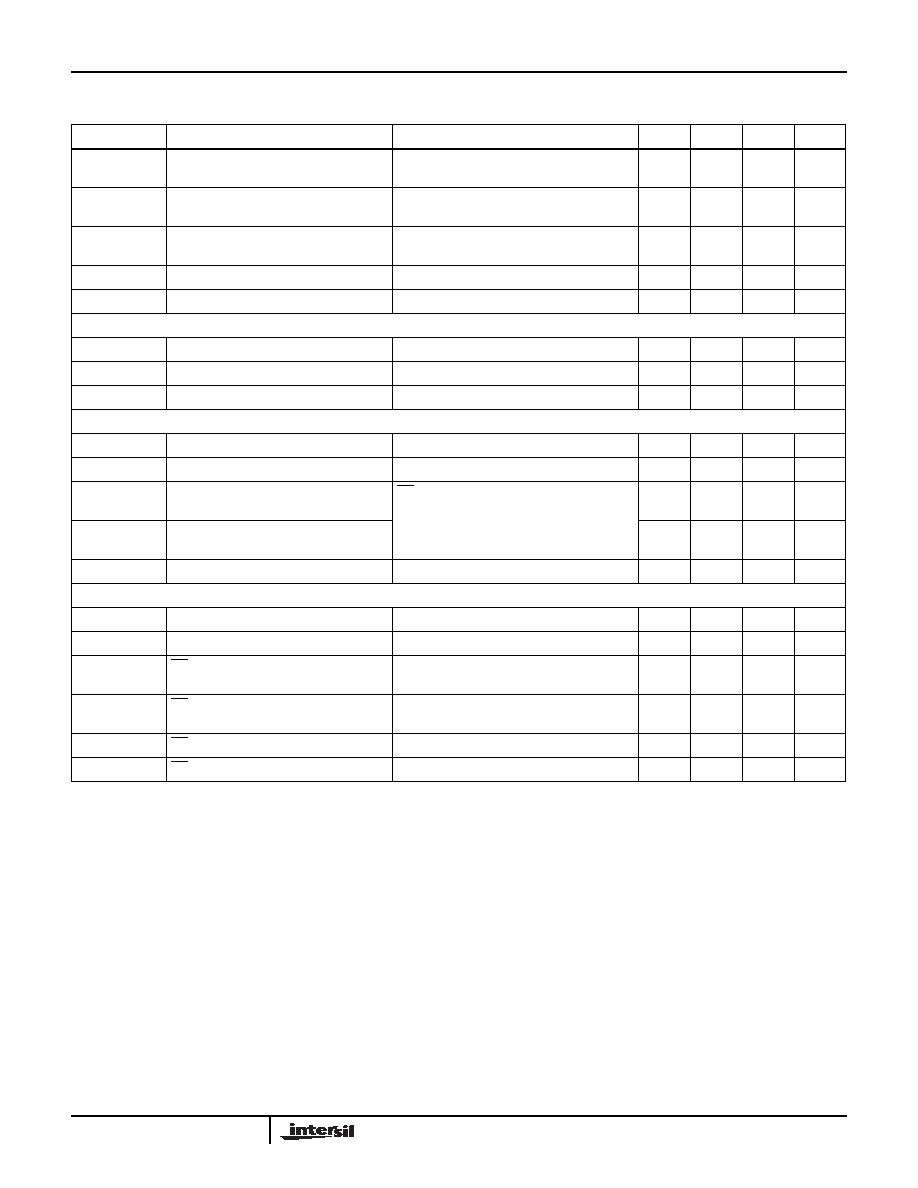
OUTPUT CHARACTERISTICS
V
OUT
Output Voltage Swing
R
L
= 1k
±3.4
±3.7
V
I
OUT
(Max)
Maximum Output Current
R
L
= 10
, V
IN
+ = ±3.2V
±50
±60
±100
mA
R
OUT
Output Impedance
130
m
SUPPLY
V
SUPPLY
Supply Operating Range
V
S
+ to V
S
-
4.75
11
V
I
S(ON)
Power Supply Current - Per Channel
10
12.5
14
mA
I
S(OFF)
+
Positive Power Supply Current - Disabled
(EL5378)
EN pin tied to 4.8V
1.7
10
µA
I
S(OFF)
-
Negative Power Supply Current -
Disabled (EL5378)
-200
-120
µA
PSRR
Power Supply Rejection Ratio
V
S
from ±4.5V to ±5.5V
60
75
dB
ENABLE (EL5378 ONLY)
t
EN
Enable Time
130
ns
t
DS
Disable Time
1.2
µs
V
IH
EN Pin Voltage for Power-Up
V
S
+ -
1.5
V
V
IL
EN Pin Voltage for Shut-Down
V
S
+ -
0.5
V
I
IH-EN
EN Pin Input Current High
At V
EN
= 5V
123
200
µA
I
IL-EN
EN Pin Input Current Low
At V
EN
= 0V
-20
-8
µA
Electrical Specifications
V
S
+ = +5V, V
S
- = -5V, T
A
= 25°C, V
IN
= 0V, R
LD
= 1k
, C
LD
= 2.7pF, [R
F
= 604
, R
G
= 402
(EL5178)],
[R
F
= 402
, R
G
= 274
(EL5378)], unless otherwise specified. (Continued)
PARAMETER
DESCRIPTION
CONDITIONS
MIN
TYP
MAX
UNIT
EL5178, EL5378
5
FN7491.1
March 8, 2005
Pin Descriptions
EL5178
EL5378
PIN NAME
PIN FUNCTION
1
17, 21, 27
FBP1, 2, 3
Feedback from non-inverting outputs
2
2, 6, 10
INP1, 2, 3
Non-inverting inputs
3
3, 7, 11
INN1, 2, 3
Inverting inputs, note that on EL5178, this pin is also the REF pin
4
16, 20, 26
FBN1, 2, 3
Feedback from inverting outputs
5
15, 19, 25
OUT1B, 2B, 3B
Inverting outputs
6
24
VSP
Positive supply
7
23
VSN
Negative supply
8
18, 22, 28
OUT1, 2, 3
Non-inverting outputs
1, 5, 9, 13
NC
No connect; grounded for best crosstalk performance
4, 8, 12
REF1, 2, 3
Reference inputs, sets common-mode output voltage
14
EN
ENABLE
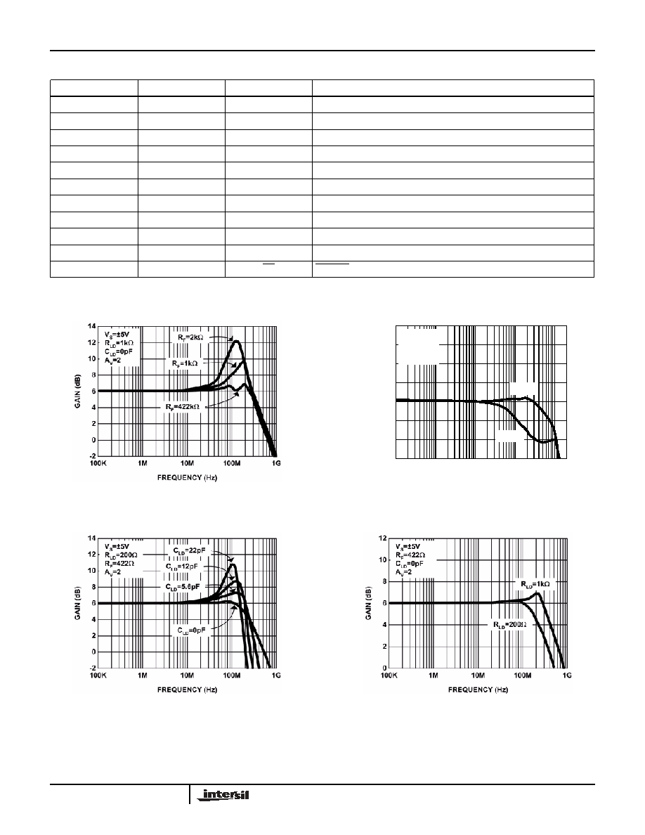
Typical Performance Curves
FIGURE 1. EL5178 FREQUENCY RESPONSE FOR VARIOUS R
F
FIGURE 2. EL5178 FREQUENCY RESPONSE FOR VARIOUS
GAIN
FIGURE 3. EL5178 FREQUENCY RESPONSE FOR VARIOUS
C
LD
FIGURE 4. EL5178 FREQUENCY RESPONSE FOR VARIOUS
R
LD
100K
1M
10M
100M
20
10
-15
FREQUENCY (Hz)
GAI
N
(
d
B)
15
5
1G
-5
0
-10
V
S
=±5V
R
LD
=1k
C
LD
=0pF
R
F
=422
A
V
=5
A
V
=2
EL5178, EL5378