
1
Æ
FN7178
CAUTION: These devices are sensitive to electrostatic discharge; follow proper IC Handling Procedures.
1-888-INTERSIL or 321-724-7143
|
Intersil (and design) is a registered trademark of Intersil Americas Inc.
Copyright © Intersil Americas Inc. 2003. All Rights Reserved. Elantec is a registered trademark of Elantec Semiconductor, Inc.
All other trademarks mentioned are the property of their respective owners.
EL5181
8ns High-Speed Comparator
The EL5181 comparator is designed
for operation in single supply and dual
supply applications with 5V to 12V
between V
S
+ and V
S
-. For single supplies, the inputs can
operate from 0.1V below ground for use in ground sensing
applications.
The output side of the comparator can be supplied from a
single supply of 2.7V to 5V. The rail-to-rail output swing
enables direct connection of the comparator to both CMOS
and TTL logic circuits.
The latch input of the EL5181 can be used to hold the com-
parator output value by applying a low logic level to the pin.
The EL5181 is available in the 8-pin SO package and is
specified for operation over the full -40∞C to +85∞C tempera-
ture range. Also available are a dual (EL5281), a window
comparator (EL5283), and quad versions (EL5481 and
EL5482).
Features
∑ 8ns Typ. propagation delay
∑ 5V to 12V input supply
∑ +2.7V to +5V output supply
∑ True-to-ground input
∑ Rail-to-rail outputs
∑ Active low latch
∑ Dual available (EL5281)
∑ Window comparator (EL5283)
∑ Quad available (EL5481 & EL5482)
∑ Pin-compatible 4ns family available (EL5x85, EL5287 &
EL5486)
Applications
∑ Threshold detection
∑ High speed sampling circuits
∑ High speed triggers
∑ Line receivers
∑ PWM circuits
∑ High speed V/F converters
Pinout
Ordering Information
PART
NUMBER
PACKAGE
TAPE & REEL
PKG. NO.
EL5181CS
8-Pin SO
-
MDP0027
EL5181CS-T7
8-Pin SO
7"
MDP0027
EL5181CS-T13
8-Pin SO
13"
MDP0027
1
2
3
4
8
7
6
5
VS+
L
A
T
C
H
VSD
OUT
GND
LATCH
IN+
IN-
VS-
-
+
EL5181
(8-PIN SO)
TOP VIEW
Data Sheet
December 4, 2001
OBSO
LETE
PRO
DUCT
NO R
ECOM
MEND
ED R
EPLA
CEME
NT
conta
ct ou
r Tec
hnica
l Sup
port C
enter
at
1-888
-INTE
RSIL
or w
ww.in
tersil
.com
/tsc
2
Absolute Maximum Ratings
(T
A
= 25∞C)
Analog Supply Voltage (V
S
+ to V
S
-) . . . . . . . . . . . . . . . . . . . +12.6V
Digital Supply Voltage (V
SD
to GND) . . . . . . . . . . . . . . . . . . . . .+7V
Differential Input Voltage . . . . . . . . . . .[(V
S
-) -0.2V] to [(V
S
+) +0.2V]
Common-mode Input Voltage . . . . . . .[(V
S
-) -0.2V] to [(V
S
+) +0.2V]
Latch Input Voltage . . . . . . . . . . . . . . . . . . . . -0.2V to [(V
SD
)
+0.2V]
Storage Temperature Range . . . . . . . . . . . . . . . . . . -65∞C to +150∞C
Ambient Operating Temperature . . . . . . . . . . . . . . . . -40∞C to +85∞C
Operating Junction Temperature . . . . . . . . . . . . . . . . . . . . . . . 125∞C
Power Dissipation . . . . . . . . . . . . . . . . . . . . . . . . . . . . . See Curves
CAUTION: Stresses above those listed in "Absolute Maximum Ratings" may cause permanent damage to the device. This is a stress only rating and operation of the
device at these or any other conditions above those indicated in the operational sections of this specification is not implied.
IMPORTANT NOTE: All parameters having Min/Max specifications are guaranteed. Typical values are for information purposes only. Unless otherwise noted, all tests
are at the specified temperature and are pulsed tests, therefore: T
J
= T
C
= T
A
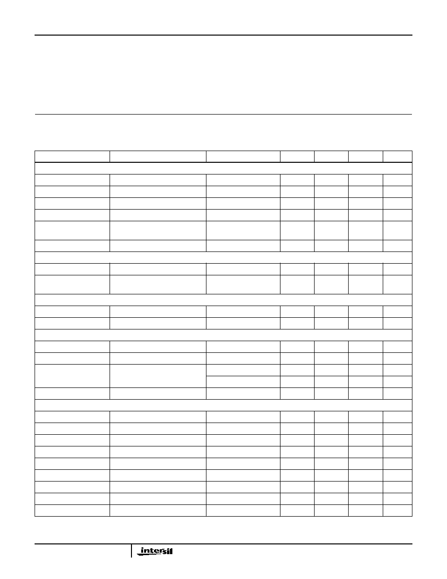
Electrical Specifications
V
S
=
±5V, V
SD
= 5V, R
L
= 2.3k
, C
L
= 15pF, T
A
= 25∞C, unless otherwise specified.
PARAMETER
DESCRIPTION
CONDITION
MIN
TYP
MAX
UNIT
INPUT
V
OS
Input Offset Voltage
V
CM
= 0V, V
O
= 2.5V
1
4
mV
I
B
Input Bias Current
-6
-3.5
µA
C
IN
Input Capacitance
5
pF
I
OS
Input Offset Current
V
CM
= 0V, V
O
= 2.5V
-2.5
0.5
2.5
µA
V
CM
Input Voltage Range
(V
S
-) - 0.1
(V
S
+) -
2.25
V
CMRR
Common-mode Rejection Ratio
-5.1V < V
CM
< +2.75V
65
90
dB
OUTPUT
V
OH
Output High Voltage
V
IN
> 250mV
V
SD
- 0.6
V
SD
- 0.4
V
V
OL
Output Low Voltage
V
IN
> 250mV
GND +
0.25
GND + 0.5
V
DYNAMIC PERFORMANCE
t
PD
+
Positive Going Delay Time
V
IN
= 1V
P-P
, V
OD
= 50mV
8
12
ns
t
PD
-
Negative Going Delay Time
V
IN
= 1V
P-P
, V
OD
= 50mV
8
12
ns
SUPPLY
I
S
+
Positive Analog Supply Current
7
8.2
mA
I
S
-
Negative Analog Supply Current
5
6.5
mA
I
SD
Digital Supply Current
Output high
4
5
mA
Output low
0.75
1
mA
PSRR
Power Supply Rejection Ratio
60
80
dB
LATCH
V
LH
Latch Input Voltage High
2.0
V
V
LL
Latch Input Voltage Low
0.8
V
I
LH
Latch Input Current High
V
LH
= 3.0V
-30
-18
µA
I
LL
Latch Input Current Low
V
LL
= 0.3V
-30
-24
µA
t
d
+
Latch Disable to High Delay
6
ns
t
D
-
Latch Disable to Low Delay
6
ns
t
S
Minimum Setup Time
2
ns
t
H
Minimum Hold Time
1
ns
t
PW
(D)
Minimum Latch Disable Pulse Width
10
ns
EL5181

3
Typical Performance Curves
Positive Supply Current vs Temperature
7.15
7.1
7.05
7
6.95
6.9
6.85
6.8
6.75
6.7
-50
-30
-10
10
30
50
70
90
Temperature (∞C)
I
S
+
(
m
A
)
Negative Supply Current vs Temperature
-4.4
-4.5
-4.6
-4.7
-4.8
-4.9
-5
-5.1
-5.2
-50
-30
-10
10
30
50
70
90
Temperature (∞C)
I
S
-
(
m
A
)
Input Bias Current vs Temperature
6
5
4
3
2
1
0
-50
-30
-10
10
30
50
70
90
Temperature (∞C)
I
B
(
µ
A
)
Offset Voltage vs Temperature
0.7
0.6
0.4
0.3
0.2
0.1
0
-0.1
-0.2
-0.3
-50
-30
-10
10
30
50
70
90
Temperature (∞C)
V
O
S
(
m
V
)
0.5
Negative Supply Current vs Negative Supply
Voltage
5.5
3
5
3.5
4.5
4
0
7
1
2
3
4
5
6
V
S
- (V)
I
S
-
(
m
A
)
7
0
5
1
3
2
I
S
+
(
m
A
)
Positive Supply Current vs Supply Voltage
0
7
1
2
3
4
5
6
V
S
+ (V)
6
4
V
S
- = -5V
V
SD
= 5V
V
IN
= 50mV
T
A
= 25∞C
V
S
+ = 5V
V
SD
= 5V
V
IN
= 50mV
T
A
= 25∞C
EL5181

4
Typical Performance Curves
(Continued)
Propagation Delay vs Supply Voltage
10
9.5
8.5
7.5
7
6.5
6
5.5
5
9
8
4
4.5
5
5.5
6
±V
S
(V)
D
e
l
a
y
T
i
m
e
(
n
s
)
T
PD
+
T
PD
-
Propagation Delay vs Overdrive
10
9.5
8.5
8
7.5
7
6.5
6
9
0
0.2
0.6
1
1.2
1.6
2
V
OD
(V)
D
e
l
a
y
T
i
m
e
(
n
s
)
T
PD
+
T
PD
-
V
S
= ±5V
V
SD
= 5V
V
IN
= 3V Step
R
L
= 2.2k
0.4
0.8
1.4
1.8
Propagation Delay vs Overdrive
11
10.5
9.5
9
8.5
8
7.5
7
10
0
0.5
1
2
3
V
OD
(V)
D
e
l
a
y
T
i
m
e
(
n
s
)
T
PD
+
T
PD
-
1.5
2.5
Propagation Delay vs Source Resistance
20
18
14
12
10
8
6
4
16
0
0.2
0.4
1
1.6
Source Resistance (k
)
D
e
l
a
y
T
i
m
e
(
n
s
)
T
PD
+
T
PD
-
0.6
1.4
1.2
0.8
Propagation Delay vs Overdrive
10
9.5
8.5
7.5
7
6.5
6
5.5
5
9
8
0
100
200
300
400
500
600
V
OD
(mV)
D
e
l
a
y
T
i
m
e
(
n
s
)
T
PD
+
T
PD
-
Propagation Delay vs Load Capacitance
12
10
9
8
7
6
11
0
20
40
60
80
100
120
C
LOAD
(pF)
D
e
l
a
y
T
i
m
e
(
n
s
)
T
PD
+
T
PD
-
V
S
= ±5V
V
SD
= 5 V
V
IN
= 1V Step
R
L
= 2.2k
V
S
= ±5V
V
SD
= 5V
R
L
= 2.2k
V
IN
= 1V Step
V
OD
= 50mV
V
SD
= V
S
+
V
IN
= 1V Step
V
OD
= 50mV
R
L
= 2.2k
V
S
= ±5V
V
SD
= 5V
R
L
= 2.2k
V
IN
= 5V Step
V
S
= ±5V
V
SD
= 5V
R
L
= 2.2k
V
IN
= 1V Step
V
OD
= 50mV
EL5181

5
Typical Performance Curves
(Continued)
0
10
2
4
6
Load Current (mA)
Output Low Voltage vs Load Current
0.31
0.15
0.27
O
u
t
p
u
t
L
o
w
V
o
l
t
a
g
e
(
V
)
8
0.23
0.19
0
10
2
4
6
Load Current (mA)
8
Output High Voltage vs Load Current
4.75
4.3
4.7
O
u
t
p
u
t
H
i
g
h
V
o
l
t
a
g
e
(
V
)
4.65
4.6
4.55
4.5
4.45
4.4
4.35
Package Power Dissipation vs Ambient Temperature
JEDEC JESD51-3 Low Effective Thermal Conductivity
Test Board
0.7
0
0.5
0.3
0.2
0.1
P
o
w
e
r
D
i
s
s
i
p
a
t
i
o
n
(
W
)
0.6
0.4
0
125
100
75
50
25
Ambient Temperature (∞C)
150
85
2V
V
IN
= 1V
P-P
F
IN
= 30MHz
1V
20ns
V
S
= ±5V
V
SD
S
= 5V
Output with 30MHz Input
V
IN
= 1V
P-P
2V
2V
20ns
V
IN
= 3V
P-P
F
IN
= 30MHz
V
S
= ±5V
V
SD
= 5V
Output with 30MHz Input
V
IN
= 3V
P-P
V
O
V
IN
V
O
V
IN
160
∞C
/W
SO
8
Digital Supply Current vs Input Switching
Frequency
30
0
25
15
10
5
I
S
D
(
m
A
)
20
0
45
35
25
15
5
Frequency (MHz)
50
40
30
20
10
V
SD
= 3V
V
S
= ±5V
V
S
= ±5V
V
SD
= 5V
V
IN
= -50mV
T
A
= -40∞C
T
A
= 25∞C
T
A
= 85∞C
T
A
= -40∞C
T
A
= 25∞C
T
A
= 85∞C
V
S
= ±5V
V
SD
= 5V
V
IN
= 50mV
V
SD
= 5V
625mW
EL5181