
1
Æ
FN7183.1
CAUTION: These devices are sensitive to electrostatic discharge; follow proper IC Handling Procedures.
1-888-INTERSIL or 321-724-7143
|
Intersil (and design) is a registered trademark of Intersil Americas Inc.
Copyright © Intersil Americas Inc. 2004. All Rights Reserved. Elantec is a registered trademark of Elantec Semiconductor, Inc.
All other trademarks mentioned are the property of their respective owners.
EL5196, EL5196A
Single 400MHz Fixed Gain Amplifier with
Enable
The EL5196 and the EL5196A are
fixed gain amplifiers with a bandwidth
of 400MHz, making these amplifiers
ideal for today's high speed video and monitor applications.
These amplifiers feature internal gain setting resistors and
can be configured in a gain of +1, -1 or +2. The same
bandwidth is seen in both gain-of-1 and gain-of-2
applications.
The EL5196A also incorporates an enable and disable
function to reduce the supply current to 100µA typical per
amplifier. Allowing the CE pin to float or applying a low logic
level will enable the amplifier.
The EL5196 is offered in the 5-pin SOT-23 package and the
EL5196A is available in the 6-pin SOT-23 as well as the
industry-standard 8-pin SO packages. Both operate over the
industrial temperature range of -40∞C to +85∞C.
Pinouts
Features
∑ Gain selectable (+1, -1, +2)
∑ 400MHz -3dB BW (A
V
= 1, 2)
∑ 9mA supply current
∑ Fast enable/disable (EL5196A only)
∑ Single and dual supply operation, from 5V to 10V or ±2.5V
to ±5V
∑ Available in SOT-23 packages
∑ Triple (EL5396) available
∑ 200MHz, 4mA products available (EL5197 & EL5397)
Applications
∑ Video amplifiers
∑ Cable drivers
∑ RGB amplifiers
∑ Test equipment
∑ Instrumentation
∑ Current to voltage converters
1
2
3
4
8
7
6
5
EL5196ACS
(8-PIN SO)
TOP VIEW
1
2
3
5
4
EL5196CW
(5-PIN SOT-23)
TOP VIEW
1
2
3
6
4
EL5196ACW
(6-PIN SOT-23)
TOP VIEW
-
+
-
+
NC
IN-
IN+
VS-
CE
VS+
OUT
NC
OUT
VS-
IN+
VS+
IN-
-
+
OUT
VS-
IN+
VS+
IN-
5
CE
Ordering Information
PART NUMBER
PACKAGE
TAPE & REEL PKG. DWG. #
EL5196CW-T7
5-Pin SOT-23
7" (3K pcs)
MDP0038
EL5196CW-T7A
5-Pin SOT-23
7" (250 pcs)
MDP0038
EL5196ACW-T7
6-Pin SOT-23
7"(3K pcs)
MDP0038
EL5196ACW-T7A 6-Pin SOT-23
7"(250 pcs)
MDP0038
EL5196ACS
8-Pin SO
-
MDP0027
EL5196ACS-T7
8-Pin SO
7"
MDP0027
EL5196ACS-T13
8-Pin SO
13"
MDP0027
Data Sheet
March 12, 2004
NOT
RECO
MME
NDED
FOR
NEW
DES
IGNS
SEE
EL51
06, E
L510
8

2
Absolute Maximum Ratings
(T
A
= 25∞C)
Supply Voltage between V
S
+ and V
S
-. . . . . . . . . . . . . . . . . . . . .11V
Maximum Continuous Output Current . . . . . . . . . . . . . . . . . . . 50mA
Operating Junction Temperature . . . . . . . . . . . . . . . . . . . . . . . 125∞C
Power Dissipation . . . . . . . . . . . . . . . . . . . . . . . . . . . . . See Curves
Pin Voltages. . . . . . . . . . . . . . . . . . . . . . . . .V
S
- - 0.5V to V
S
+ +0.5V
Storage Temperature. . . . . . . . . . . . . . . . . . . . . . . .-65∞C to +150∞C
Operating Ambient Temperature . . . . . . . . . . . . . . . .-40∞C to +85∞C
CAUTION: Stresses above those listed in "Absolute Maximum Ratings" may cause permanent damage to the device. This is a stress only rating and operation of the
device at these or any other conditions above those indicated in the operational sections of this specification is not implied.
IMPORTANT NOTE: All parameters having Min/Max specifications are guaranteed. Typical values are for information purposes only. Unless otherwise noted, all tests
are at the specified temperature and are pulsed tests, therefore: T
J
= T
C
= T
A
Electrical Specifications
V
S
+ = +5V, V
S
- = -5V, R
L
= 150
, T
A
= 25∞C unless otherwise specified.
PARAMETER
DESCRIPTION
CONDITIONS
MIN
TYP
MAX
UNIT
AC PERFORMANCE
BW
-3dB Bandwidth
A
V
= +1
400
MHz
A
V
= -1
400
MHz
A
V
= +2
400
MHz
BW1
0.1dB Bandwidth
35
MHz
SR
Slew Rate
V
O
= -2.5V to +2.5V, A
V
= +2
2400
2900
V/µs
t
S
0.1% Settling Time
V
OUT
= -2.5V to +2.5V, AV = -1
9
ns
e
N
Input Voltage Noise
3.8
nV/
Hz
i
N
-
IN- Input Current Noise
25
pA/
Hz
i
N
+
IN+ Input Current Noise
55
pA/
Hz
dG
Differential Gain Error (Note 1)
A
V
= +2
0.035
%
dP
Differential Phase Error (Note 2)
A
V
= +2
0.04
∞
DC PERFORMANCE
V
OS
Offset Voltage
-15
1
15
mV
T
C
V
OS
Input Offset Voltage Temperature
Coefficient
Measured from T
MIN
to T
MAX
5
µV/∞C
A
E
Gain Error
V
O
= -3V to +3V
-2
1.3
2
%
R
F
, R
G
Internal R
F
and R
G
320
400
480
INPUT CHARACTERISTICS
CMIR
Common Mode Input Range
±3V
±3.3V
V
+I
IN
+ Input Current
-120
40
120
µA
-I
IN
- Input Current
-40
4
40
µA
R
IN
Input Resistance
at I
N
+
27
k
C
IN
Input Capacitance
0.5
pF
OUTPUT CHARACTERISTICS
V
O
Output Voltage Swing
R
L
= 150
to GND
±3.4V
±3.7V
V
R
L
= 1k
to GND
±3.8V
±4.0V
V
I
OUT
Output Current
R
L
= 10
to GND
95
120
mA
SUPPLY
I
SON
Supply Current - Enabled
No load, V
IN
= 0V
8
9
11
mA
I
SOFF
Supply Current - Disabled
No load, V
IN
= 0V
100
150
µA
PSRR
Power Supply Rejection Ratio
DC, V
S
= ±4.75V to ±5.25V
55
75
dB
EL5196, EL5196A
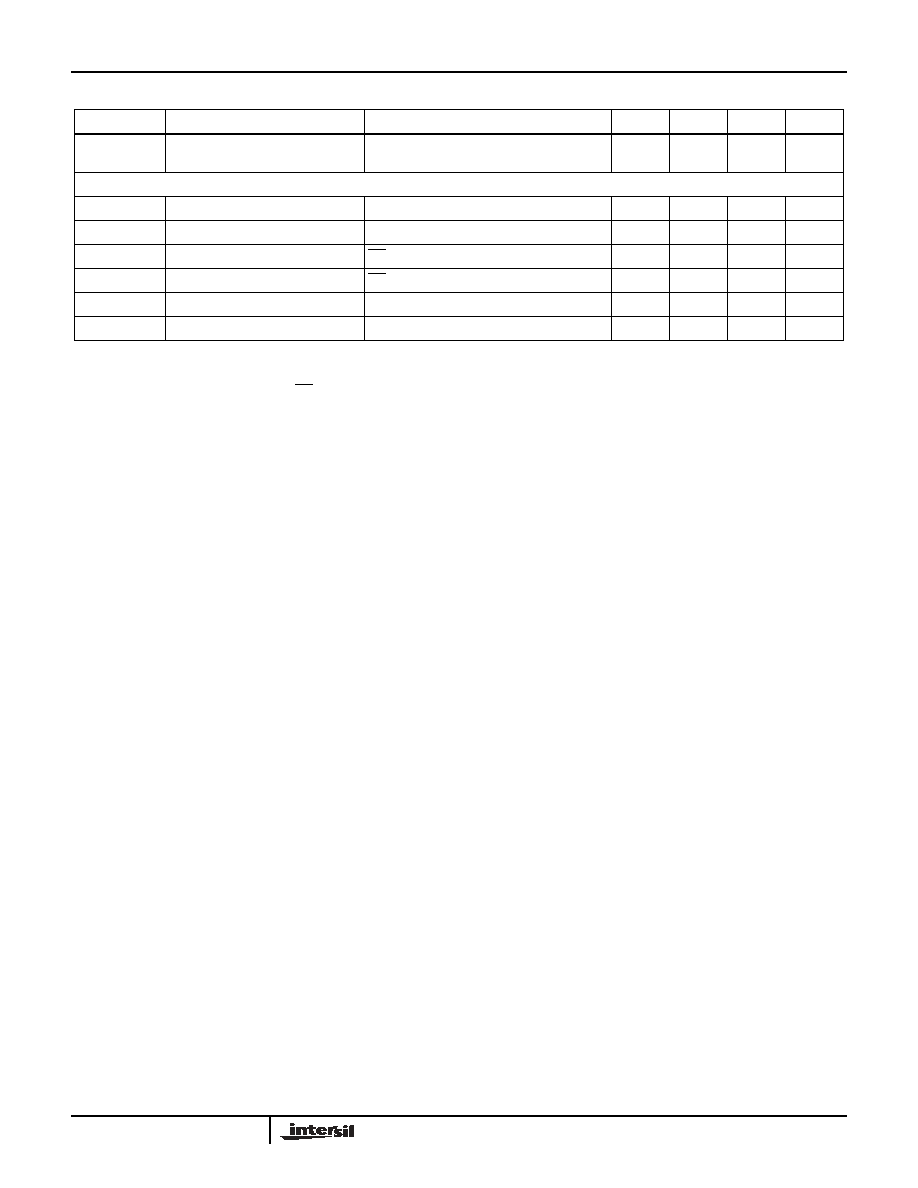
3
-IPSR
- Input Current Power Supply
Rejection
DC, V
S
= ±4.75V to ±5.25V
-2
2
µA/V
ENABLE (EL5196A ONLY)
t
EN
Enable Time
40
ns
t
DIS
Disable Time
600
ns
I
IHCE
CE Pin Input High Current
CE = V
S
+
0.8
6
µA
I
ILCE
CE Pin Input Low Current
CE = V
S
-
0
-0.1
µA
V
IHCE
CE Input High Voltage for Disable
V
S
+ - 1
V
V
ILCE
CE Input Low Voltage for Enable
V
S
+ - 3
V
NOTES:
1. Standard NTSC test, AC signal amplitude = 286mV
P-P
, f = 3.58MHz.
2. Measured from the application of the CE logic signal until the output voltage is at the 50% point between initial and final values.
Electrical Specifications
V
S
+ = +5V, V
S
- = -5V, R
L
= 150
, T
A
= 25∞C unless otherwise specified. (Continued)
PARAMETER
DESCRIPTION
CONDITIONS
MIN
TYP
MAX
UNIT
EL5196, EL5196A
4
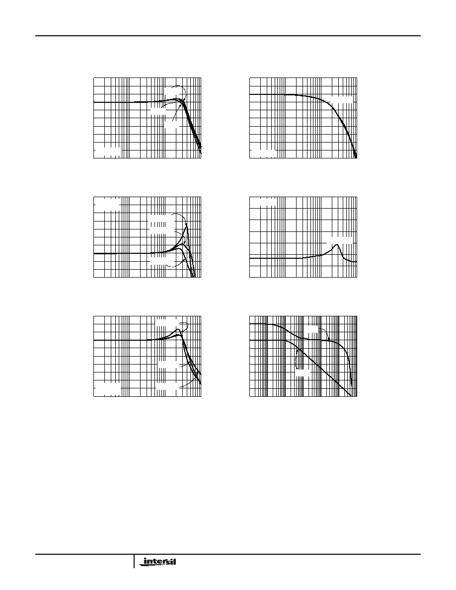
Typical Performance Curves
Frequency Response (Gain)
SOT-23 Package
1M
10M
100M
1G
2
-2
-6
-10
-14
Frequency (Hz)
N
o
rm
alize
d
Magnitude (dB)
A
V
= -1
A
V
= 1
Frequency Response (Phase)
SOT-23 Package
1M
10M
100M
1G
90
0
-90
-180
-270
-360
Frequency (Hz)
P
h
as
e (
∞
)
R
L
= 150
All Gains
6
A
V
= 2
Frequency Response for Various C
L
1M
10M
100M
1G
Frequency (Hz)
Norma
lized M
a
gnitu
de
(dB)
8pF added
4pF added
0pF added
A
V
= 2
R
L
= 150
Group Delay vs Frequency, All Gains
1M
10M
100M
1G
-3.5
-3
-2.5
-1.5
-0.5
0
Frequency (Hz)
De
l
a
y
(
n
s)
R
L
= 150
All Gains
Frequency Response for Various Common-Mode
Input Voltages
1M
10M
100M
1G
Frequency (Hz)
No
r
m
ali
z
ed Magnitude
(
d
B)
V
CM
= 3V
V
CM
= 0V
V
CM
= -3V
A
V
= 2
R
L
= 150
-2
-1
10
6
2
-2
-6
14
2
-2
-6
-10
-14
6
Transimpedance (ROL) vs Frequency
1k
Frequency (Hz)
10k
100k
1M
10M
100M
1G
10M
100
1k
10k
100k
1M
Magnitude (
)
-90
-180
-270
-360
0
Ph
as
e (∞
)
R
L
= 150
Phase
ROL
EL5196, EL5196A
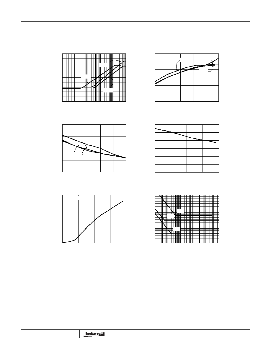
5
Typical Performance Curves
(Continued)
PSRR and CMRR vs Frequency
P
S
RR/CMRR (
d
B)
Frequency (Hz)
20
-80
-60
-40
-20
0
10k
100k
1M
10M
1G
100M
-3dB Bandwidth vs Supply Voltage
5
6
7
10
450
400
350
300
Total Supply Voltage (V)
-
3
dB
Ba
ndw
i
d
th
(MH
z)
A
V
=2
A
V
=-1
A
V
=1
R
L
=150
Peaking vs Supply Voltage
4
3
2
1
0
Total Supply Voltage (V)
P
e
a
k
ing (dB)
A
V
= 2
A
V
= -1
A
V
= 1
R
L
= 150
C
LOAD
= 0pF
8
9
5
6
7
10
8
9
Voltage and Current Noise vs Frequency
100
Frequency (Hz)
1k
10k
100k
10M
1M
i
N
+
i
N
-
e
N
V
o
lt
age N
o
i
s
e
(nV
/
Hz)
Current
Noise
(
p
A/
Hz)
1k
1
10
100
-3dB Bandwidth vs Temperature
-40
10
60
160
600
500
300
100
0
Ambient Temperature (∞C)
-3dB Ba
n
d
w
i
dth
(
M
Hz)
R
L
= 150
Peaking vs Temperature
0.6
0.5
0.4
0.2
0
Ambient Temperature (∞C)
Pe
ak
ing (dB
)
R
L
= 150
110
400
200
-40
10
60
160
110
0.3
0.1
PSRR+
PSRR1
CMRR
EL5196, EL5196A