Äîêóìåíòàöèÿ è îïèñàíèÿ www.docs.chipfind.ru
1
®
FN7187.1
EL5221
Dual 12MHz Rail-to-Rail Input-Output
Buffer
The EL5221 is a dual, low power, high voltage rail-to-rail
input-output buffer. Operating on supplies ranging from 5V to
15V, while consuming only 500µA per channel, the EL5221
has a bandwidth of 12MHz
-
(-3dB). The EL5221 also
provides rail-to-rail input and output ability, giving the
maximum dynamic range at any supply voltage.
The EL5221 also features fast slewing and settling times, as
well as a high output drive capability of 30mA (sink and
source). These features make the EL5221 ideal for use as
voltage reference buffers in Thin Film Transistor Liquid
Crystal Displays (TFT-LCD). Other applications include
battery power, portable devices, and anywhere low power
consumption is important.
The EL5221 is available in space-saving 6-pin SOT-23 and
8-pin MSOP packages and operates over a temperature
range of -40°C to +85°C.
Features
· 12MHz -3dB bandwidth
· Unity gain buffer
· Supply voltage = 4.5V to 16.5V
· Low supply current (per buffer) = 500µA
· High slew rate = 10V/µs
· Rail-to-rail operation
·
Pb-Free plus anneal available (RoHS compliant)
Applications
· TFT-LCD drive circuits
· Electronics notebooks
· Electronics games
· Personal communication devices
· Personal Digital Assistants (PDA)
· Portable instrumentation
· Wireless LANs
· Office automation
· Active filters
· ADC/DAC buffer
Pinouts
EL5221
(6-PIN SOT-23)
TOP VIEW
EL5221
(8-PIN MSOP)
TOP VIEW
Ordering Information
PART NUMBER
PACKAGE
TAPE &
REEL
PKG. DWG. #
EL5221CW-T7
6-Pin SOT-23*
7" (3K pcs)
MDP0038
EL5221CW-T7A
6-Pin SOT-23*
7" (250 pcs)
MDP0038
EL5221CWZ-T7
(See Note)
6-Pin SOT-23*
(Pb-free)
7" (3K pcs)
MDP0038
EL5221CWZ-T7A
(See Note)
6-Pin SOT-23*
(Pb-free)
7" (250 pcs)
MDP0038
EL5221CY
8-Pin MSOP
-
MDP0043
EL5221CY-T7
8-Pin MSOP
7"
MDP0043
EL5221CY-T13
8-Pin MSOP
13"
MDP0043
EL5221CYZ
(See Note)
8-Pin MSOP
(Pb-free)
-
MDP0043
EL5221CYZ-T7
(See Note)
8-Pin MSOP
(Pb-free)
7"
MDP0043
EL5221CYZ-T13
(See Note)
8-Pin MSOP
(Pb-free)
13"
MDP0043
*EL5221CW symbol is .Mxxx where xxx represents date code
.
NOTE: Intersil Pb-free plus anneal products employ special Pb-free
material sets; molding compounds/die attach materials and 100%
matte tin plate termination finish, which are RoHS compliant and
compatible with both SnPb and Pb-free soldering operations. Intersil
Pb-free products are MSL classified at Pb-free peak reflow
temperatures that meet or exceed the Pb-free requirements of
IPC/JEDEC J STD-020.
VINA
VS-
VINB
1
2
3
6
5
4
VOUTA
VOUTB
VS+
VS+
NC
VOUTB
1
2
3
4
8
7
6
5
VOUTA
NC
VINA
VINB
VS-
Data Sheet
August 2, 2005
CAUTION: These devices are sensitive to electrostatic discharge; follow proper IC Handling Procedures.
1-888-INTERSIL or 1-888-468-3774
|
Intersil (and design) is a registered trademark of Intersil Americas Inc.
Copyright Intersil Americas Inc. 2002, 2005. All Rights Reserved
All other trademarks mentioned are the property of their respective owners.
2
Absolute Maximum Ratings
(T
A
= 25°C)
Supply Voltage between V
S
+ and V
S
-. . . . . . . . . . . . . . . . . . . .+18V
Input Voltage . . . . . . . . . . . . . . . . . . . . . . . . . V
S
- - 0.5V, V
S
+ +0.5V
Maximum Continuous Output Current . . . . . . . . . . . . . . . . . . . 30mA
Maximum Die Temperature . . . . . . . . . . . . . . . . . . . . . . . . . . +125°C
Storage Temperature. . . . . . . . . . . . . . . . . . . . . . . .-65°C to +150°C
Operating Temperature . . . . . . . . . . . . . . . . . . . . . . .-40°C to +85°C
Power Dissipation . . . . . . . . . . . . . . . . . . . . . . . . . . . . . See Curves
ESD Voltage . . . . . . . . . . . . . . . . . . . . . . . . . . . . . . . . . . . . . . . . 2kV
CAUTION: Stresses above those listed in "Absolute Maximum Ratings" may cause permanent damage to the device. This is a stress only rating and operation of the
device at these or any other conditions above those indicated in the operational sections of this specification is not implied.
IMPORTANT NOTE: All parameters having Min/Max specifications are guaranteed. Typical values are for information purposes only. Unless otherwise noted, all tests
are at the specified temperature and are pulsed tests, therefore: T
J
= T
C
= T
A
Electrical Specifications
V
S
+ = +5V, V
S
- = -5V, R
L
= 10k
and C
L
= 10pF to 0V, T
A
= 25°C unless otherwise specified.
PARAMETER
DESCRIPTION
CONDITION
MIN
TYP
MAX
UNIT
INPUT CHARACTERISTICS
V
OS
Input Offset Voltage
V
CM
= 0V
2
12
mV
TCV
OS
Average Offset Voltage Drift
(Note 1)
5
µV/°C
I
B
Input Bias Current
V
CM
= 0V
2
50
nA
R
IN
Input Impedance
1
G
C
IN
Input Capacitance
1.35
pF
A
V
Voltage Gain
-4.5V
V
OUT
4.5V
0.995
1.005
V/V
OUTPUT CHARACTERISTICS
V
OL
Output Swing Low
I
L
= -5mA
-4.92
-4.85
V
V
OH
Output Swing High
I
L
= 5mA
4.85
4.92
V
I
SC
Short Circuit Current
Short to GND
±120
mA
POWER SUPPLY PERFORMANCE
PSRR
Power Supply Rejection Ratio
V
S
is moved from ±2.25V to ±7.75V
60
80
dB
I
S
Supply Current (Per Buffer)
No load
500
750
µA
DYNAMIC PERFORMANCE
SR
Slew Rate (Note 2)
-4.0V
V
OUT
4.0V, 20% to 80%
7
10
V/µs
t
S
Settling to +0.1%
V
O
= 2V step
500
ns
BW
-3dB Bandwidth
R
L
= 10k
, C
L
= 10pF
12
MHz
CS
Channel Separation
f = 5MHz
75
dB
NOTES:
1. Measured over the operating temperature range
2. Slew rate is measured on rising and falling edges
EL5221
3
Electrical Specifications
V
S
+ = +5V, V
S
- = 0V, R
L
= 10k
and C
L
= 10pF to 2.5V, T
A
= 25°C unless otherwise specified.
PARAMETER
DESCRIPTION
CONDITION
MIN
TYP
MAX
UNIT
INPUT CHARACTERISTICS
V
OS
Input Offset Voltage
V
CM
= 2.5V
2
10
mV
TCV
OS
Average Offset Voltage Drift
(Note 1)
5
µV/°C
I
B
Input Bias Current
V
CM
= 2.5V
2
50
nA
R
IN
Input Impedance
1
G
C
IN
Input Capacitance
1.35
pF
A
V
Voltage Gain
0.5
V
OUT
4.5V
0.995
1.005
V/V
OUTPUT CHARACTERISTICS
V
OL
Output Swing Low
I
L
= -5mA
80
150
mV
V
OH
Output Swing High
I
L
= 5mA
4.85
4.92
V
I
SC
Short Circuit Current
Short to GND
±120
mA
POWER SUPPLY PERFORMANCE
PSRR
Power Supply Rejection Ratio
V
S
is moved from 4.5V to 15.5V
60
80
dB
I
S
Supply Current (Per Buffer)
No Load
500
750
µA
DYNAMIC PERFORMANCE
SR
Slew Rate (Note 2)
1V
V
OUT
4V, 20% to 80%
7
10
V/µs
t
S
Settling to +0.1%
V
O
= 2V Step
500
ns
BW
-3dB Bandwidth
R
L
= 10k
, C
L
= 10pF
12
MHz
CS
Channel Separation
f = 5MHz
75
dB
NOTES:
1. Measured over the operating temperature range
2. Slew rate is measured on rising and falling edges
EL5221

4
Electrical Specifications
V
S
+ = +15V, V
S
- = 0V, R
L
= 10k
and C
L
= 10pF to 7.5V, T
A
= 25°C unless otherwise specified.
PARAMETER
DESCRIPTION
CONDITION
MIN
TYP
MAX
UNIT
INPUT CHARACTERISTICS
V
OS
Input Offset Voltage
V
CM
= 7.5V
2
14
mV
TCV
OS
Average Offset Voltage Drift
(Note 1)
5
µV/°C
I
B
Input Bias Current
V
CM
= 7.5V
2
50
nA
R
IN
Input Impedance
1
G
C
IN
Input Capacitance
1.35
pF
A
V
Voltage Gain
0.5
V
OUT
14.5V
0.995
1.005
V/V
OUTPUT CHARACTERISTICS
V
OL
Output Swing Low
I
L
= -5mA
80
150
mV
V
OH
Output Swing High
I
L
= 5mA
14.85
14.92
V
I
SC
Short Circuit Current
Short to GND
±120
mA
POWER SUPPLY PERFORMANCE
PSRR
Power Supply Rejection Ratio
V
S
is moved from 4.5V to 15.5V
60
80
dB
I
S
Supply Current (Per Buffer)
No Load
500
750
µA
DYNAMIC PERFORMANCE
SR
Slew Rate (Note 2)
1V
V
OUT
14V, 20% to 80%
7
10
V/µs
t
S
Settling to +0.1%
V
O
= 2V Step
500
ns
BW
-3dB Bandwidth
R
L
= 10k
, C
L
= 10pF
12
MHz
CS
Channel Separation
f = 5MHz
75
dB
NOTES:
1. Measured over the operating temperature range
2. Slew rate is measured on rising and falling edges
EL5221
5
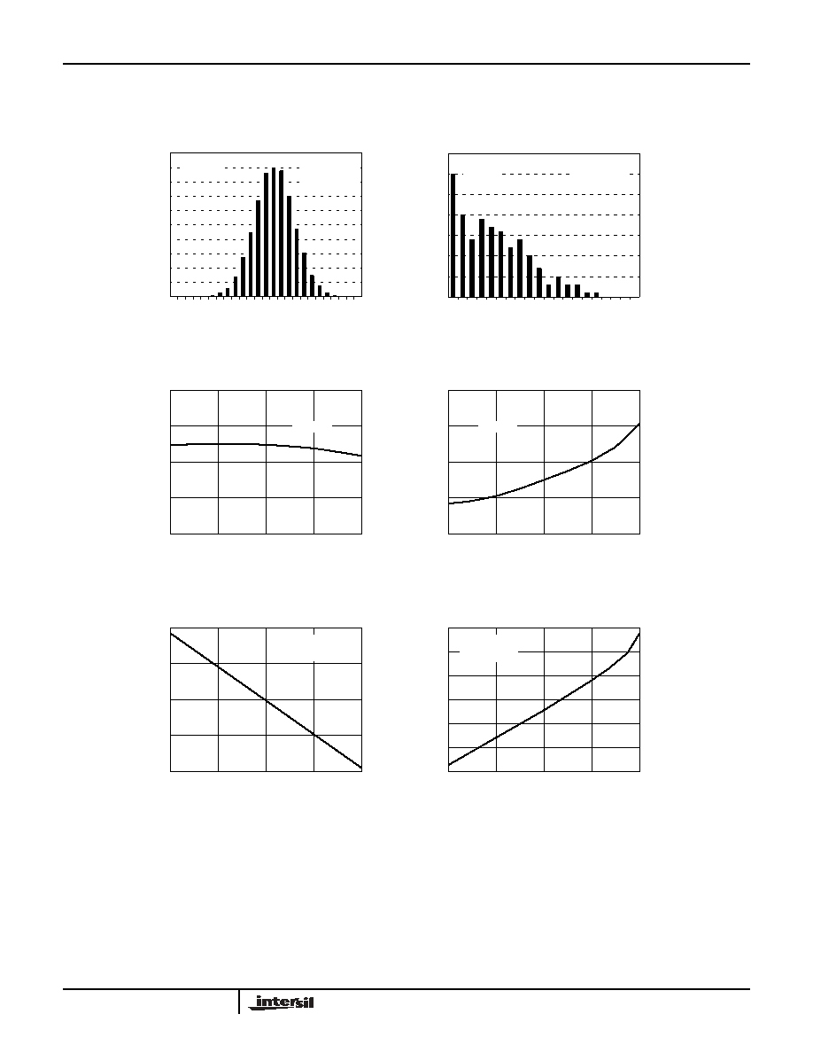
Typical Performance Curves
Input Offset Voltage Distribution
Q
uan
tity (
B
u
ffe
rs)
Input Offset Voltage (mV)
0
-1
2
2000
400
1600
1200
800
-1
0
-8
-6
-4
-2
0
2
4
6
8
10
12
Input Bias Current vs Temperature
In
pu
t Bia
s
Cur
r
e
n
t
(n
A)
Temperature (°C)
Output Low Voltage vs Temperature
O
u
tp
u
t
L
o
w
V
o
lt
ag
e (V
)
Temperature (°C)
Output High Voltage vs Temperature
Ou
tp
ut H
i
g
h
Vo
l
t
ag
e (
V
)
Temperature (°C)
Input Offset Voltage vs Temperature
0
150
0
5
Inp
u
t
Offse
t
V
o
ltag
e
(m
V)
Temperature (°C)
-10
50
-50
100
10
Typical
Production
Distribution
V
S
=±5V
T
A
=25°C
Input Offset Voltage Drift
Typical
Production
Distribution
V
S
=±5V
T
A
=25°C
Input Offset Voltage, TCVOS (µV/°C)
1
3
5
7
9
11
13
15
17
19
Qua
n
tity
(B
uff
e
r
s
)
0
35
5
30
20
10
25
15
V
S
=±5V
-5
0
-2
2
4
-4
0
150
50
-50
100
V
S
=±5V
4.97
4.96
4.95
4.94
4.93
-50
0
50
100
150
V
S
=±5V
I
OUT
=5mA
-4.95
-4.93
-4.97
-4.91
-4.92
-4.94
-4.96
0
150
50
-50
100
V
S
=±5V
I
OUT
=-5mA
EL5221