 | –≠–ª–µ–∫—Ç—Ä–æ–Ω–Ω—ã–π –∫–æ–º–ø–æ–Ω–µ–Ω—Ç: EL5250CS | –°–∫–∞—á–∞—Ç—å:  PDF PDF  ZIP ZIP |

1
Æ
FN7384.1
CAUTION: These devices are sensitive to electrostatic discharge; follow proper IC Handling Procedures.
1-888-INTERSIL or 321-724-7143
|
Intersil (and design) is a registered trademark of Intersil Americas Inc.
Copyright © Intersil Americas Inc. 2004. All Rights Reserved. Elantec is a registered trademark of Elantec Semiconductor, Inc.
All other trademarks mentioned are the property of their respective owners.
P R E L I M I N A RY
EL5150, EL5151, EL5250, EL5251, EL5451
200MHz Amplifiers
The EL5150, EL5151, EL5250,
EL5251, and EL5451 are 200MHz
bandwidth -3dB voltage mode
feedback amplifiers with DC accuracy of 0.01%, 1mV offsets
and 10kV/V open loop gains. These amplifiers are ideally
suited for applications ranging from precision measurement
instrumentation to high speed video and monitor
applications. Capable of operating with as little as 1.4mA of
current from a single supply ranging from 5V to 12V dual
supplies ranging from ±2.5V to ±5.0V, these amplifiers are
also well suited for handheld, portable and battery-powered
equipment.
Single amplifiers are offered in SOT-23 packages and duals
in a 10-pin MSOP package for applications where board
space is critical. Quad amplifiers are available in a 14-pin SO
package. Additionally, singles and duals are available in the
industry-standard 8-pin SO package. All parts operate over
the industrial temperature range of -40∞C to +85∞C.
Features
∑ 200MHz -3dB bandwidth
∑ 110V/µs slew rate
∑ Very high open loop gains 50kV/V
∑ Low supply current = 1.4mA
∑ Single supplies from 5V to 12V
∑ Dual supplies from ±2.5V to ±5V
∑ Fast disable on the EL5150 and EL5250
∑ Low cost
Applications
∑ Imaging
∑ Instrumentation
∑ Video
∑ Communications devices
Ordering Information
PART
NUMBER
PACKAGE
TAPE & REEL
PKG. DWG. #
EL5150IS
8-Pin SO
-
MDP0027
EL5150IS-T7
8-Pin SO
7"
MDP0027
EL5150IS-T13
8-Pin SO
13"
MDP0027
EL5150IW-T7
6-Pin SOT-23
7" (3K pcs)
MDP0038
EL5150IW-T7A
6-Pin SOT-23
7" (250 pcs)
MDP0038
EL5151IW-T7
5-Pin SOT-23
7" (3K pcs)
MDP0038
EL5151IW-T7A
5-Pin SOT-23
7" (250 pcs)
MDP0038
EL5250IY
10-Pin MSOP
-
MDP0043
EL5250IY-T7
10-Pin MSOP
7"
MDP0043
EL5250IY-T13
10-Pin MSOP
13"
MDP0043
EL5251IS
8-Pin SO
-
MDP0027
EL5251IS-T7
8-Pin SO
7"
MDP0027
EL5251IS-T13
8-Pin SO
13"
MDP0027
EL5251IY
8-Pin MSOP
-
MDP0043
EL5251IY-T7
8-Pin MSOP
7"
MDP0043
EL5251IY-T13
8-Pin MSOP
13"
MDP0043
EL5451IS
14-Pin SO
-
MDP0027
EL5451IS-T7
14-Pin SO
7"
MDP0027
EL5451IS-T13
14-Pin SO
13"
MDP0027
Data Sheet
February 26, 2004

2
Pinouts
EL5150
(8-PIN SO)
TOP VIEW
EL5150
(6-PIN SOT-23)
TOP VIEW
EL5151
(5-PIN SOT-23)
TOP VIEW
EL5250
(10-PIN MSOP)
TOP VIEW
EL5251
(8-PIN MSOP)
TOP VIEW
EL5451
(14-PIN SO)
TOP VIEW
1
2
3
4
8
7
6
5
-
+
NC
IN-
IN+
VS-
CE
VS+
OUT
NC
1
2
3
6
4
5
-
+
OUT
VS-
IN+
VS+
IN-
CE
1
2
3
5
4
-
+
OUT
VS-
IN+
VS+
IN-
1
2
3
4
10
9
8
7
5
6
-
+
-
+
INA+
CEA
VS-
CEB
INA-
OUTA
VS+
OUTB
INB+
INB-
1
2
3
4
8
7
6
5
-
+
-
+
OUTA
INA-
INA+
VS-
VS+
OUTB
INB-
INB+
OUTA
INA-
INA+
VS+
OUTD
IND-
IND+
VS-
INB+
INC+
1
2
3
4
14
13
12
11
5
6
7
10
9
8
INC-
OUTC
INB-
OUTB
- +
-
+
- +
-
+
EL5150, EL5151, EL5250, EL5251, EL5451

3
Absolute Maximum Ratings
(T
A
= 25∞C)
Supply Voltage between V
S
and GND . . . . . . . . . . . . . . . . . . . . .12V
Maximum Continuous Output Current . . . . . . . . . . . . . . . . . . . 40mA
Pin Voltages . . . . . . . . . . . . . . . . . . . . . . . . . GND -0.5V to V
S
+0.5V
Power Dissipation . . . . . . . . . . . . . . . . . . . . . . . . . . . . . See Curves
Junction Temperature . . . . . . . . . . . . . . . . . . . . . . . -40∞C to +125∞C
Storage Temperature . . . . . . . . . . . . . . . . . . . . . . . . -65∞C to +150∞C
Ambient Operating Temperature . . . . . . . . . . . . . . . . -40∞C to +85∞C
Current into I
N
+, I
N
-, CE . . . . . . . . . . . . . . . . . . . . . . . . . . . . . . 5mA
CAUTION: Stresses above those listed in "Absolute Maximum Ratings" may cause permanent damage to the device. This is a stress only rating and operation of the
device at these or any other conditions above those indicated in the operational sections of this specification is not implied.
IMPORTANT NOTE: All parameters having Min/Max specifications are guaranteed. Typical values are for information purposes only. Unless otherwise noted, all tests
are at the specified temperature and are pulsed tests, therefore: T
J
= T
C
= T
A
Electrical Specifications
V
S
+ = +5V, V
S
- = ±5V, R
L
= 150
, T
A
= 25∞C, unless otherwise specified.
PARAMETER
DESCRIPTION
CONDITIONS
MIN
TYP
MAX
UNIT
AC PERFORMANCE
BW
-3dB Bandwidth
A
V
= +1, R
L
= 500
200
MHz
A
V
= +2, R
L
= 150
36
MHz
GBWP
Gain Bandwidth Product
A
V
= 500
86
MHz
BW1
0.1dB Bandwidth
A
V
= +1, R
L
= 500
10
MHz
SR
Slew Rate
V
O
= ±2.5V, A
V
= +2
50
67
V/µs
V
O
= ±3.0V, A
V
= 1, R
L
= 500
100
V/µs
t
S
0.1% Settling Time
V
OUT
= -1V to +1V, A
V
= -2
80
ns
dG
Differential Gain Error (Note 1)
A
V
= +2, R
L
= 150
0.1
%
dP
Differential Phase Error (Note 1)
A
V
= +2, R
L
= 150
1.17
∞
V
N
Input Referred Voltage Noise
12
nV/
Hz
I
N
Input Referred Current Noise
1.6
pA/
Hz
DC PERFORMANCE
V
OS
Offset Voltage
-1
0.5
1
mV
T
C
V
OS
Input Offset Voltage Temperature
Coefficient
Measured from T
MIN
to T
MAX
-2
µV/∞C
A
VOL
Open Loop Gain
15
56
kV/V
INPUT CHARACTERISTICS
CMIR
Common Mode Input Range
Guaranteed by CMRR test
TBD
TBD
V
CMRR
Common Mode Rejection Ratio
85
100
dB
I
B
Input Bias Current
-100
20
+100
mA
I
OS
Input Offset Current
-30
6
30
nA
R
IN
Input Resistance
80
170
M
C
IN
Input Capacitance
1
pF
OUTPUT CHARACTERISTICS
V
OUT
Output Voltage Swing Low
R
L
= 150
to GND
±2.5
±2.8
V
R
L
= 500
to GND
±3.1
±3.4
V
I
OUT
Output Current
R
L
= 10
to GND
±40
±70
mA
ENABLE (SELECTED PACKAGES ONLY)
t
EN
Enable Time
170
ns
t
DIS
Disable Time
1.25
µs
I
IHCE
CE Pin Input High Current
CE = V
S
+
0
-1
µA
EL5150, EL5151, EL5250, EL5251, EL5451
4
All Intersil U.S. products are manufactured, assembled and tested utilizing ISO9000 quality systems.
Intersil Corporation's quality certifications can be viewed at www.intersil.com/design/quality
Intersil products are sold by description only. Intersil Corporation reserves the right to make changes in circuit design, software and/or specifications at any time without
notice. Accordingly, the reader is cautioned to verify that data sheets are current before placing orders. Information furnished by Intersil is believed to be accurate and
reliable. However, no responsibility is assumed by Intersil or its subsidiaries for its use; nor for any infringements of patents or other rights of third parties which may result
from its use. No license is granted by implication or otherwise under any patent or patent rights of Intersil or its subsidiaries.
For information regarding Intersil Corporation and its products, see www.intersil.com
I
ILCE
CE Pin Input Low Current
CE = V
S
-
5
13
25
µA
V
IHCE
CE Input High Voltage for Power-down
V
S
+ -1
V
V
ILCE
CE Input Low Voltage for Power-down
V
S
+ -3
V
SUPPLY
I
SON
Supply Current - Enabled (per amplifier)
No load, V
IN
= 0V, CE = +5V
1.12
1.35
1.6
mA
I
SOFF
Supply Current - Disabled
No load, V
IN
= 0V
5
13
25
µA
PSRR
Power Supply Rejection Ratio
DC, V
S
= ±3.0V to ±6.0V
80
110
dB
NOTE:
1. Standard NTSC test, AC signal amplitude = 286mV
P-P
, f = 3.58MHz, V
OUT
is swept from 0.8V to 3.4V, R
L
is DC coupled
Electrical Specifications
V
S
+ = +5V, V
S
- = ±5V, R
L
= 150
, T
A
= 25∞C, unless otherwise specified. (Continued)
PARAMETER
DESCRIPTION
CONDITIONS
MIN
TYP
MAX
UNIT
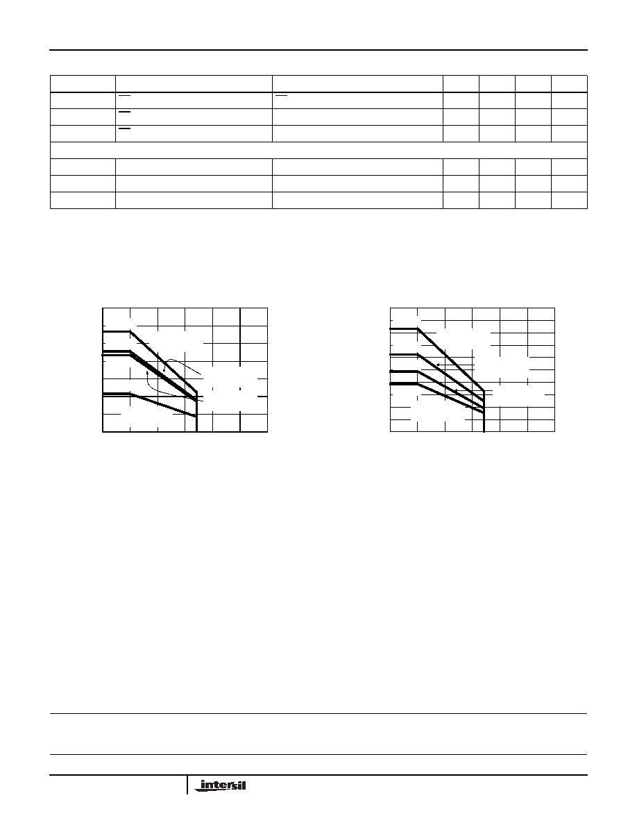
Typical Performance Curves
FIGURE 1. PACKAGE POWER DISSIPATION vs AMBIENT
TEMPERATURE
FIGURE 2. PACKAGE POWER DISSIPATION vs AMBIENT
TEMPERATURE
1.136W
909mW
JA
=110∞C/W
SO8
JA
=88∞C/W
SO14
1.4
1.2
1
0.8
0.6
0.2
0
0
25
50
75
100
150
AMBIENT TEMPERATURE (∞C)
PO
WE
R DI
SSI
PAT
I
O
N
(
W
)
125
85
JEDEC JESD51-7 HIGH EFFECTIVE THERMAL
CONDUCTIVITY TEST BOARD
0.4
870mW
435mW
JA
=230∞C/W
SOT23-5/6
JA
=115∞C/W
MSOP8/10
833mW
625mW
JA
=120∞C/W
SO14
1
0.9
0.8
0.6
0.4
0.1
0
0
25
50
75
100
150
AMBIENT TEMPERATURE (∞C)
PO
WE
R DI
SSI
PAT
I
O
N
(
W
)
125
85
JEDEC JESD51-3 LOW EFFECTIVE THERMAL
CONDUCTIVITY TEST BOARD
0.2
0.7
0.3
0.5
391mW
JA
=265∞C/W
SOT23-5/6
486mW
JA
=160∞C/W
SO8
JA
=206∞C/W
MSOP8/10
EL5150, EL5151, EL5250, EL5251, EL5451