1
Æ
FN7195.1
CAUTION: These devices are sensitive to electrostatic discharge; follow proper IC Handling Procedures.
1-888-INTERSIL or 321-724-7143
|
Intersil (and design) is a registered trademark of Intersil Americas Inc.
Copyright © Intersil Americas Inc. 2004. All Rights Reserved. Elantec is a registered trademark of Elantec Semiconductor, Inc.
All other trademarks mentioned are the property of their respective owners.
EL5393A
Triple 300MHz Current Feedback Amplifier
with Enable
The EL5393A is a triple current
feedback amplifier with a bandwidth of
300MHz. This makes these amplifiers
ideal for today's high speed video and monitor applications.
With a supply current of just 4mA per amplifier and the ability
to run from a single supply voltage from 5V to 10V, these
amplifiers are also ideal for hand held, portable or battery
powered equipment.
The EL5393A also incorporates an enable and disable
function to reduce the supply current to 100µA typical per
amplifier. Allowing the CE pin to float or applying a low logic
level will enable the amplifier.
For applications where board space is critical, the EL5393A
is offered in 16-pin QSOP package, as well as an industry
standard 16-pin SO (0.150"). The EL5393A operates over
the industrial temperature range of -40
∞
C to +85
∞
C.
Features
∑ 300MHz -3dB bandwidth
∑ 4mA supply current (per amplifier)
∑ Single and dual supply operation, from 5V to 10V
∑ Fast enable/disable
∑ Available in 16-pin QSOP package
∑ Single (EL5193) and dual (EL5293) available
∑ High speed, 1GHz product available (EL5191)
∑ High speed, 6mA, 600MHz product available (EL5192,
EL5292, and EL5392)
Applications
∑ Battery-powered equipment
∑ Hand-held, portable devices
∑ Video amplifiers
∑ Cable drivers
∑ RGB amplifiers
∑ Test equipment
∑ Instrumentation
∑ Current to voltage converters
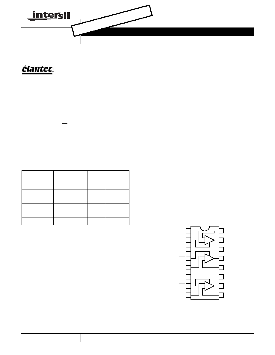
Pinout
Ordering Information
PART NUMBER
PACKAGE
TAPE &
REEL
PKG. NO.
EL5393ACS
16-Pin SO (0.150")
-
MDP0027
EL5393ACS-T7
16-Pin SO (0.150")
7"
MDP0027
EL5393ACS-T13
16-Pin SO (0.150")
13"
MDP0027
EL5393ACU
16-Pin QSOP
-
MDP0040
EL5393ACU-T7
16-Pin QSOP
7"
MDP0040
EL5393ACU-T13
16-Pin QSOP
13"
MDP0040
1
2
3
4
16
15
14
13
5
6
7
12
11
10
8
9
-
+
-
+
-
+
INA+
CEA
VS-
CEB
INB+
NC
CEC
INC+
INA-
OUTA
VS+
OUTB
INB-
NC
OUTC
INC-
EL5393A
[16-PIN SO (0.150"), QSOP]
TOP VIEW
Data Sheet
January 22, 2004
NOT
REC
OMM
END
ED F
OR
NEW
DES
IGNS
SEE
EL5
360,
EL5
362

2
Absolute Maximum Ratings
(T
A
= 25∞C)
Supply Voltage between V
S
+ and V
S
- . . . . . . . . . . . . . . . . . . . . . 11V
Maximum Continuous Output Current . . . . . . . . . . . . . . . . . . . 50mA
Operating Junction Temperature . . . . . . . . . . . . . . . . . . . . . . . 125∞C
Power Dissipation . . . . . . . . . . . . . . . . . . . . . . . . . . . . . See Curves
Pin Voltages. . . . . . . . . . . . . . . . . . . . . . . . . V
S
- -0.5V to V
S
+ +0.5V
Storage Temperature . . . . . . . . . . . . . . . . . . . . . . . . -65∞C to +150∞C
Ambient Operating Temperature . . . . . . . . . . . . . . . . -40∞C to +85∞C
CAUTION: Stresses above those listed in "Absolute Maximum Ratings" may cause permanent damage to the device. This is a stress only rating and operation of the
device at these or any other conditions above those indicated in the operational sections of this specification is not implied.
IMPORTANT NOTE: All parameters having Min/Max specifications are guaranteed. Typical values are for information purposes only. Unless otherwise noted, all tests
are at the specified temperature and are pulsed tests, therefore: T
J
= T
C
= T
A
Electrical Specifications
V
S
+ = +5V, V
S
- = -5V, R
F
= 750
for A
V
= 1, R
F
= 375
for A
V
= 2, R
L
= 150
, T
A
= 25∞C unless otherwise
specified.
PARAMETER
DESCRIPTION
CONDITIONS
MIN
TYP
MAX
UNIT
AC PERFORMANCE
BW
-3dB Bandwidth
A
V
= +1
300
MHz
A
V
= +2
200
MHz
BW1
0.1dB Bandwidth
20
MHz
SR
Slew Rate
V
O
= -2.5V to +2.5V, A
V
= +2
1900
2200
V/µs
t
S
0.1% Settling Time
V
OUT
= -2.5V to +2.5V, A
V
= -1
12
ns
C
S
Channel Separation
f = 5MHz
60
dB
e
N
Input Voltage Noise
4.4
nV/
Hz
i
N
-
IN- Input Current Noise
17
pA/
Hz
i
N
+
IN+ Input Current Noise
50
pA/
Hz
dG
Differential Gain Error (Note 1)
A
V
= +2
0.03
%
dP
Differential Phase Error (Note 1)
A
V
= +2
0.04
∞
DC PERFORMANCE
V
OS
Offset Voltage
-10
1
10
mV
T
C
V
OS
Input Offset Voltage Temperature
Coefficient
Measured from T
MIN
to T
MAX
5
µV/∞C
R
OL
Transimpedance
300
600
k
INPUT CHARACTERISTICS
CMIR
Common Mode Input Range
±3
±3.3
V
CMRR
Common Mode Rejection Ratio
42
50
dB
+I
IN
+ Input Current
-60
1
80
µA
-I
IN
- Input Current
-35
1
35
µA
R
IN
Input Resistance
45
k
C
IN
Input Capacitance
0.5
pF
OUTPUT CHARACTERISTICS
V
O
Output Voltage Swing
R
L
= 150
to GND
±3.4
±3.7
V
R
L
= 1k
to GND
±3.8
±4.0
V
I
OUT
Output Current
R
L
= 10
to GND
95
120
mA
SUPPLY
I
SON
Supply Current - Enabled
No load, V
IN
= 0V
3
4
5
mA
I
SOFF
Supply Current - Disabled
No load, V
IN
= 0V
100
150
µA
EL5393A
3
PSRR
Power Supply Rejection Ratio
DC, V
S
= ±4.75V to ±5.25V
55
75
dB
-IPSR
- Input Current Power Supply Rejection
DC, V
S
= ±4.75V to ±5.25V
-2
2
µA/V
ENABLE
t
EN
Enable Time
40
ns
t
DIS
Disable Time
600
ns
I
IHCE
CE Pin Input High Current
CE = V
S
+
0.8
6
µA
I
ILCE
CE Pin Input Low Current
CE = V
S
-
0
-0.1
µA
V
IHCE
CE Input High Voltage for Power-down
V
S
+ -1
V
V
ILCE
CE Input Low Voltage for Power-down
V
S
+ -3
V
NOTE:
1. Standard NTSC test, AC signal amplitude = 286mV
P-P
, f = 3.58MHz.
Electrical Specifications
V
S
+ = +5V, V
S
- = -5V, R
F
= 750
for A
V
= 1, R
F
= 375
for A
V
= 2, R
L
= 150
, T
A
= 25∞C unless otherwise
specified. (Continued)
PARAMETER
DESCRIPTION
CONDITIONS
MIN
TYP
MAX
UNIT
EL5393A

4
Typical Performance Curves
Non-Inverting Frequency Response (Gain)
1M
10M
100M
1G
6
2
-2
-6
-10
-14
Frequency (Hz)
N
o
r
m
alize
d
M
a
g
n
itu
d
e (
d
B)
A
V
=2
A
V
=5
A
V
=10
A
V
=1
R
F
=750
R
L
=150
Non-Inverting Frequency Response (Phase)
1M
10M
100M
1G
90
0
-90
-180
-270
-360
Frequency (Hz)
P
h
a
se (∞
)
A
V
=2
A
V
=5
A
V
=10
A
V
=1
R
F
=750
R
L
=150
Inverting Frequency Response (Gain)
1M
10M
100M
1G
6
2
-2
-6
-10
-14
Frequency (Hz)
No
r
m
a
lized
Mag
n
it
u
d
e
(d
B)
A
V
=-2
A
V
=-3
A
V
=-1
R
F
=500
R
L
=150
Inverting Frequency Response (Phase)
1M
10M
100M
1G
90
0
-90
-180
-270
-360
Frequency (Hz)
P
h
ase (
∞
)
A
V
=-2
A
V
=-3
A
V
=-1
R
F
=500
R
L
=150
Frequency Response for Various R
L
1M
10M
100M
1G
6
2
-2
-6
-10
-14
Frequency (Hz)
No
r
m
alized
Mag
n
it
u
d
e (d
B)
A
V
=2
R
F
=500
R
L
=100
R
L
=500
R
L
=150
Frequency Response for Various C
IN
-
1M
10M
100M
1G
10
6
2
-2
-6
-10
Frequency (Hz)
No
r
m
alized
Mag
n
it
u
d
e (d
B)
0pF added
2pF added
1pF added
A
V
=2
R
F
=500
R
L
=150
EL5393A

5
Typical Performance Curves
(Continued)
Frequency Response for Various C
L
1M
10M
100M
1G
14
10
6
2
-2
-6
Frequency (Hz)
No
r
m
alized
Ma
g
n
itu
d
e (
d
B)
A
V
=2
R
L
=150
R
F
=R
G
=500
33pF
22pF
15pF
8pF
0pF
Group Delay vs Frequency
1M
10M
100M
1G
Frequency (Hz)
D
e
lay (
n
s)
A
V
=1
R
F
=750
A
V
=2
R
F
=500
Frequency Response for Various Common-Mode
Input Voltages
1M
10M
100M
1G
6
2
-2
-6
-10
-14
Frequency (Hz)
N
o
r
m
ali
z
ed M
a
gn
itu
d
e
(dB
)
A
V
=2
R
F
=500
R
L
=150
V
CM
=3V
V
CM
=0V
V
CM
=-3V
3.5
0
3
2.5
2
1.5
1
0.5
Frequency Response for Various R
F
1M
10M
100M
1G
6
2
-2
-6
-10
-14
Frequency (Hz)
No
r
m
alized
Ma
g
n
itu
d
e (
d
B)
A
V
=2
R
G
=R
F
R
L
=150
340
475
620
750
1.2k
Transimpedance (ROL) vs Frequency
1k
Frequency (Hz)
10k
100k
1M
10M
100M
1G
10M
100
1k
10k
100k
1M
Phase
PSRR and CMRR vs Frequency
PSRR/CM
RR (
d
B)
Frequency (Hz)
Mag
n
i
t
ud
e (
)
20
-80
-60
-40
-20
0
10k
100k
1M
10M
1G
100M
-90
-180
-270
-360
0
P
h
ase (
∞
)
Gain
PSRR+
PSRR-
CMRR
EL5393A