 | ÐлекÑÑоннÑй компоненÑ: EL5421CY | СкаÑаÑÑ:  PDF PDF  ZIP ZIP |
Äîêóìåíòàöèÿ è îïèñàíèÿ www.docs.chipfind.ru
1
®
FN7198.1
CAUTION: These devices are sensitive to electrostatic discharge; follow proper IC Handling Procedures.
1-888-INTERSIL or 321-724-7143
|
Intersil (and design) is a registered trademark of Intersil Americas Inc.
Copyright © Intersil Americas Inc. 2004. All Rights Reserved. Elantec is a registered trademark of Elantec Semiconductor, Inc.
All other trademarks mentioned are the property of their respective owners.
EL5421
Quad 12MHz Rail-to-Rail Input-Output
Buffer
The EL5421 is a quad, low power, high
voltage rail-to-rail input-output buffer.
Operating on supplies ranging from 5V
to 15V, while consuming only 500µA per channel, the
EL5421 has a bandwidth of 12MHz (-3dB). The EL5421 also
provides rail-to-rail input and output ability, giving the
maximum dynamic range at any supply voltage.
The EL5421 also features fast slewing and settling times, as
well as a high output drive capability of 30mA (sink and
source). These features make the EL5421 ideal for use as
voltage reference buffers in Thin Film Transistor Liquid
Crystal Displays (TFT-LCD). Other applications include
battery power, portable devices and anywhere low power
consumption is important.
The EL5421 is available in a space saving 10-pin MSOP
package and operates over a temperature range of -40°C to
+85°C.
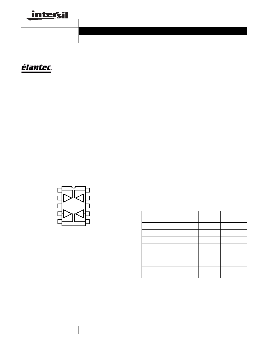
Pinout
EL 5421
(10-PIN MSOP)
TOP VIEW
Features
· 12MHz -3dB bandwidth
· Unity gain buffer
· Supply voltage = 4.5V to 16.5V
· Low supply current (per buffer) = 500µA
· High slew rate = 10V/µs
· Rail-to-rail operation
· "Mini" SO package (MSOP)
· Pb-free package available
Applications
· TFT-LCD drive circuits
· Electronics notebooks
· Electronics games
· Personal communication devices
· Personal digital assistants (PDA)
· Portable instrumentation
· Wireless LANs
· Office automation
· Active filters
· ADC/DAC buffers
1
2
3
4
10
9
8
7
5
6
VOUTA
VINA
VS+
VINB
VOUTB
VOUTD
VIND
VS-
VINC
VOUTC
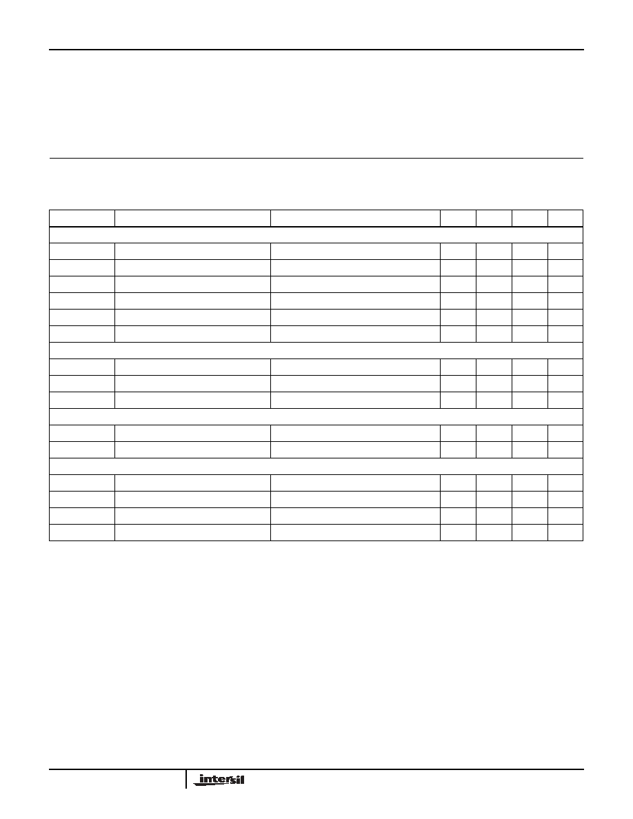
Ordering Information
PART NUMBER
PACKAGE
TAPE &
REEL
PKG. DWG. #
EL5421CY
10-Pin MSOP
-
MDP0043
EL5421CY-T7
10-Pin MSOP
7"
MDP0043
EL5421CY-T13
10-Pin MSOP
13"
MDP0043
EL5421CYZ
(Note)
10-Pin MSOP
(Pb-Free)
-
MDP0043
EL5421CYZ-T7
(Note)
10-Pin MSOP
(Pb-Free)
7"
MDP0043
EL5421CYZ-T13
(Note)
10-Pin MSOP
(Pb-Free)
13"
MDP0043
NOTE: Intersil Pb-free products employ special Pb-free material
sets; molding compounds/die attach materials and 100% matte tin
plate termination finish, which is compatible with both SnPb and
Pb-free soldering operations. Intersil Pb-free products are MSL
classified at Pb-free peak reflow temperatures that meet or exceed
the Pb-free requirements of IPC/JEDEC J Std-020B.
Data Sheet
June 14, 2004
2
Absolute Maximum Ratings
(T
A
= 25
°
C)
Supply Voltage between V
S
+ and V
S
- . . . . . . . . . . . . . . . . . . . .+18V
Input Voltage . . . . . . . . . . . . . . . . . . . . . . . . . . V
S
- -0.5V, V
S
+ +0.5V
Maximum Continuous Output Current . . . . . . . . . . . . . . . . . . . 30mA
Maximum Die Temperature . . . . . . . . . . . . . . . . . . . . . . . . . . +125°C
Storage Temperature . . . . . . . . . . . . . . . . . . . . . . . .-65°C to +150°C
Operating Temperature . . . . . . . . . . . . . . . . . . . . . . .-40°C to +85°C
Power Dissipation . . . . . . . . . . . . . . . . . . . . . . . . . . . . . See Curves
CAUTION: Stresses above those listed in "Absolute Maximum Ratings" may cause permanent damage to the device. This is a stress only rating and operation of the
device at these or any other conditions above those indicated in the operational sections of this specification is not implied.
IMPORTANT NOTE: All parameters having Min/Max specifications are guaranteed. Typical values are for information purposes only. Unless otherwise noted, all tests
are at the specified temperature and are pulsed tests, therefore: T
J
= T
C
= T
A
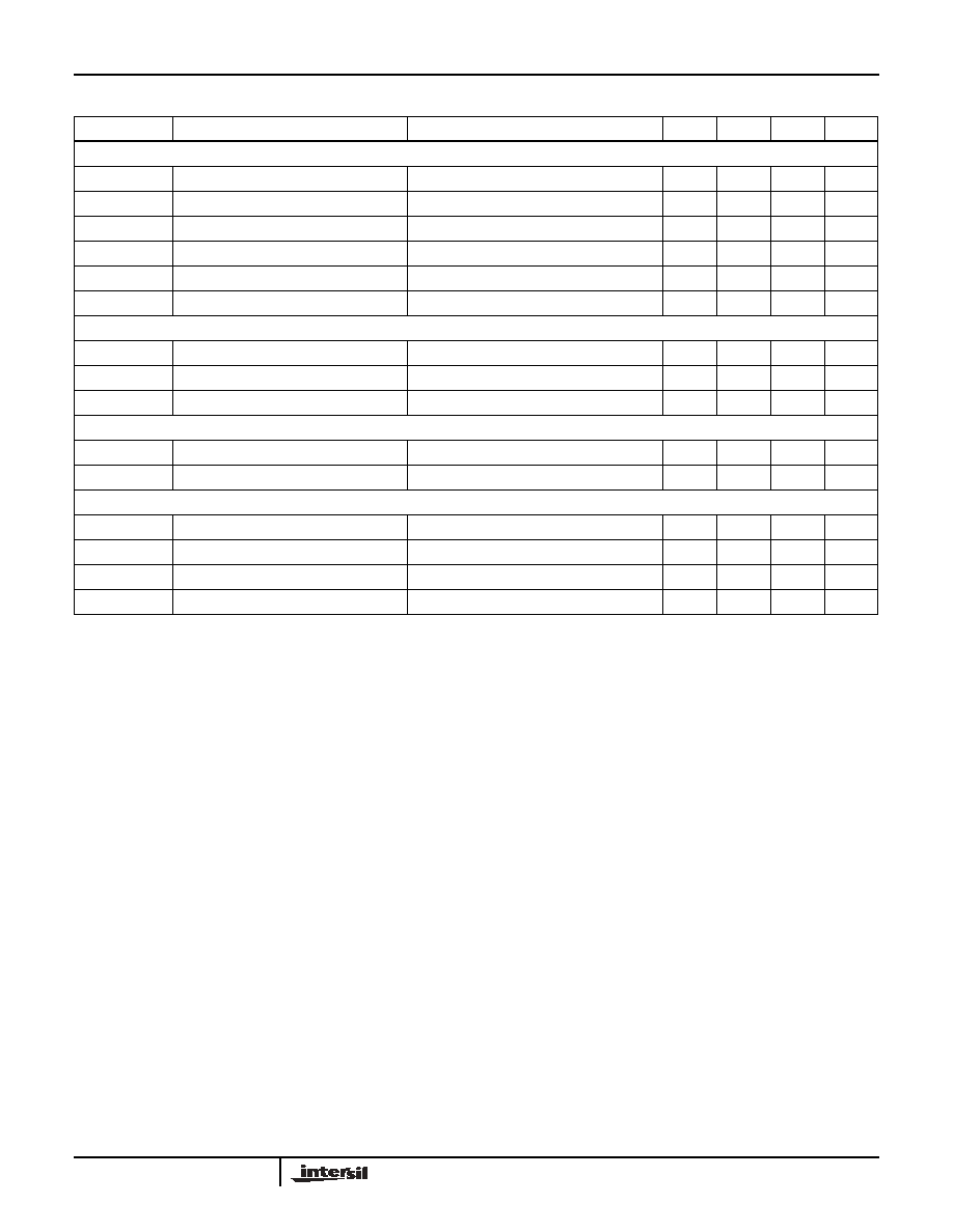
Electrical Specifications
V
S
+ = +5V, V
S
- = -5V, R
L
= 10k
and C
L
= 10pF to 0V, T
A
= 25°C unless otherwise specified.
PARAMETER
DESCRIPTION
CONDITION
MIN
TYP
MAX
UNIT
INPUT CHARACTERISTICS
V
OS
Input Offset Voltage
V
CM
= 0V
2
12
mV
TCV
OS
Average Offset Voltage Drift
(Note 1)
5
µV/°C
I
B
Input Bias Current
V
CM
= 0V
2
50
nA
R
IN
Input Impedance
1
G
C
IN
Input Capacitance
1.35
pF
A
V
Voltage Gain
-4.5V
V
OUT
4.5V
0.995
1.005
V/V
OUTPUT CHARACTERISTICS
V
OL
Output Swing Low
I
L
= -5mA
-4.92
-4.85
V
V
OH
Output Swing High
I
L
= 5mA
4.85
4.92
V
I
SC
Short Circuit Current
Short to GND (Note 2)
±80
±120
mA
POWER SUPPLY PERFORMANCE
PSRR
Power Supply Rejection Ratio
V
S
is moved from ±2.25V to ±7.75V
60
80
dB
I
S
Supply Current (Per Buffer)
No load
500
750
µA
DYNAMIC PERFORMANCE
SR
Slew Rate (Note 3)
-4.0V
V
OUT
4.0V, 20% to 80%
7
10
V/µs
t
S
Settling to +0.1%
V
O
= 2V step
500
ns
BW
-3dB Bandwidth
R
L
= 10k
, C
L
= 10pF
12
MHz
CS
Channel Separation
f = 5MHz
75
dB
NOTES:
1. Measured over the operating temperature range
2. Parameter is guaranteed (but not test) by design and characterization data
3. Slew rate is measured on rising and falling edges
EL5421
3
Electrical Specifications
V
S
+ = +5V, V
S
- = 0V, R
L
= 10k
and C
L
= 10pF to 2.5V, T
A
= 25°C unless otherwise specified.
PARAMETER
DESCRIPTION
CONDITION
MIN
TYP
MAX
UNIT
INPUT CHARACTERISTICS
V
OS
Input Offset Voltage
V
CM
= 2.5V
2
10
mV
TCV
OS
Average Offset Voltage Drift
(Note 1)
5
µV/°C
I
B
Input Bias Current
V
CM
= 2.5V
2
50
nA
R
IN
Input Impedance
1
G
C
IN
Input Capacitance
1.35
pF
A
V
Voltage Gain
0.5
V
OUT
4.5V
0.995
1.005
V/V
OUTPUT CHARACTERISTICS
V
OL
Output Swing Low
I
L
= -5mA
80
150
mV
V
OH
Output Swing High
I
L
= 5mA
4.85
4.92
V
I
SC
Short Circuit Current
Short to GND (Note 2)
±80
±120
mA
POWER SUPPLY PERFORMANCE
PSRR
Power Supply Rejection Ratio
V
S
is moved from 4.5V to 15.5V
60
80
dB
I
S
Supply Current (Per Buffer)
No load
500
750
µA
DYNAMIC PERFORMANCE
SR
Slew Rate (Note 3)
1V
V
OUT
4V, 20% to 80%
7
10
V/µs
t
S
Settling to +0.1%
V
O
= 2V step
500
ns
BW
-3dB Bandwidth
R
L
= 10k
, C
L
= 10pF
12
MHz
CS
Channel Separation
f = 5MHz
75
dB
NOTES:
1. Measured over the operating temperature range
2. Parameter is guaranteed (but not test) by design and characterization data
3. Slew rate is measured on rising and falling edges
EL5421

4
Electrical Specifications
V
S
+ = +15V, V
S
- = 0V, R
L
= 10k
and C
L
= 10pF to 7.5V, T
A
= 25°C unless otherwise specified.
PARAMETER
DESCRIPTION
CONDITION
MIN
TYP
MAX
UNIT
INPUT CHARACTERISTICS
V
OS
Input Offset Voltage
V
CM
= 7.5V
2
14
mV
TCV
OS
Average Offset Voltage Drift
(Note 1)
5
µV/°C
I
B
Input Bias Current
V
CM
= 7.5V
2
50
nA
R
IN
Input Impedance
1
G
C
IN
Input Capacitance
1.35
pF
A
V
Voltage Gain
0.5
V
OUT
14.5V
0.995
1.005
V/V
OUTPUT CHARACTERISTICS
V
OL
Output Swing Low
I
L
= -5mA
80
150
mV
V
OH
Output Swing High
I
L
= 5mA
14.85
14.92
V
I
SC
Short Circuit Current
Short to GND (Note 2)
±80
±120
mA
POWER SUPPLY PERFORMANCE
PSRR
Power Supply Rejection Ratio
V
S
is moved from 4.5V to 15.5V
60
80
dB
I
S
Supply Current (Per Buffer)
No load
500
750
µA
DYNAMIC PERFORMANCE
SR
Slew Rate (Note 3)
1V
V
OUT
14V, 20% to 80%
7
10
V/µs
t
S
Settling to +0.1%
V
O
= 2V step
500
ns
BW
-3dB Bandwidth
R
L
= 10k
, C
L
= 10pF
12
MHz
CS
Channel Separation
f = 5MHz
75
dB
NOTES:
1. Measured over the operating temperature range
2. Parameter is guaranteed (but not test) by design and characterization data
3. Slew rate is measured on rising and falling edges
EL5421
5
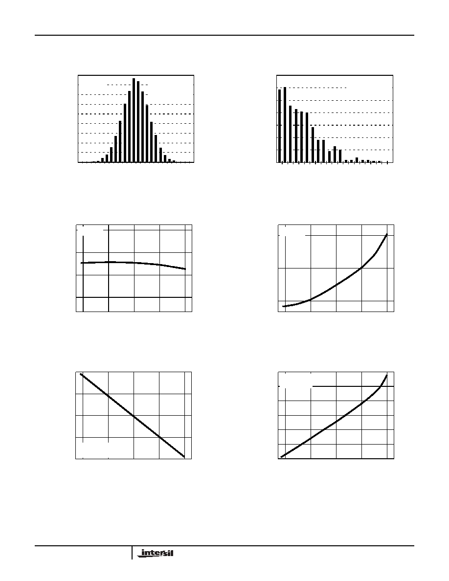
Typical Performance Curves
FIGURE 1. INPUT OFFSET VOLTAGE DISTRIBUTION
FIGURE 2. INPUT OFFSET VOLTAGE DRIFT
FIGURE 3. INPUT OFFSET VOLTAGE vs TEMPERATURE
FIGURE 4. INPUT BIAS CURRENT vs TEMPERATURE
FIGURE 5. OUTPUT HIGH VOLTGE vs TEMPERATURE
FIGURE 6. OUTPUT LOW VOLTAGE vs TEMPERATURE
400
1200
QUANTITY (BUFFERS)
INPUT OFFSET VOLTAGE (mV)
0
-12
1800
1600
800
200
1400
1000
600
-10
-8
-6
-4
-2
-0
2
4
6
8
10
12
TYPICAL
PRODUCTION
DISTRIBUTION
V
S
=±5V
T
A
=25°C
INPUT OFFSET VOLTAGE DRIFT, TCV
OS
(µV/°C)
1
3
5
7
9
11
13
15
17
19
21
10
50
QUANTITY (BUFFERS)
0
70
30
60
40
20
V
S
=±5V
TYPICAL
PRODUCTION
DISTRIBUTION
0
150
0
5
I
N
PUT OFFSET VOLTAGE
(m
V)
TEMPERATURE (°C)
-5
50
-50
100
10
V
S
=±5V
0.0
INPUT
BIAS C
URRENT (nA)
-2.0
2.0
V
S
=±5V
0
150
TEMPERATURE (°C)
50
-50
100
4.94
4.95
OUT
P
UT
HI
GH
VOL
T
A
GE
(
V
)
4.93
4.97
4.96
0
150
TEMPERATURE (°C)
50
-50
100
V
S
=±5V
I
OUT
=5mA
-4.95
-4.93
O
U
TPUT LO
W VO
LTAG
E
(V)
-4.97
-4.91
-4.92
-4.94
-4.96
V
S
=±5V
I
OUT
=-5mA
0
150
TEMPERATURE (°C)
50
-50
100
EL5421