 | ÐлекÑÑоннÑй компоненÑ: EL5462 | СкаÑаÑÑ:  PDF PDF  ZIP ZIP |
Äîêóìåíòàöèÿ è îïèñàíèÿ www.docs.chipfind.ru
1
®
FN7492.0
CAUTION: These devices are sensitive to electrostatic discharge; follow proper IC Handling Procedures.
1-888-INTERSIL or 321-724-7143
|
Intersil (and design) is a registered trademark of Intersil Americas Inc.
Copyright © Intersil Americas Inc. 2005. All Rights Reserved.
All other trademarks mentioned are the property of their respective owners.
EL5462
500MHz Low Power Current Feedback
Amplifier
The EL5462 is a current feedback amplifier with a bandwidth
of 500MHz which makes this amplifier ideal for today's high
speed video and monitor applications.
With a supply current of just 1.5mA per amplifier and the
ability to run from a single supply voltage from 5V to 12V, the
EL5462 is also ideal for handheld, portable or battery-
powered equipment.
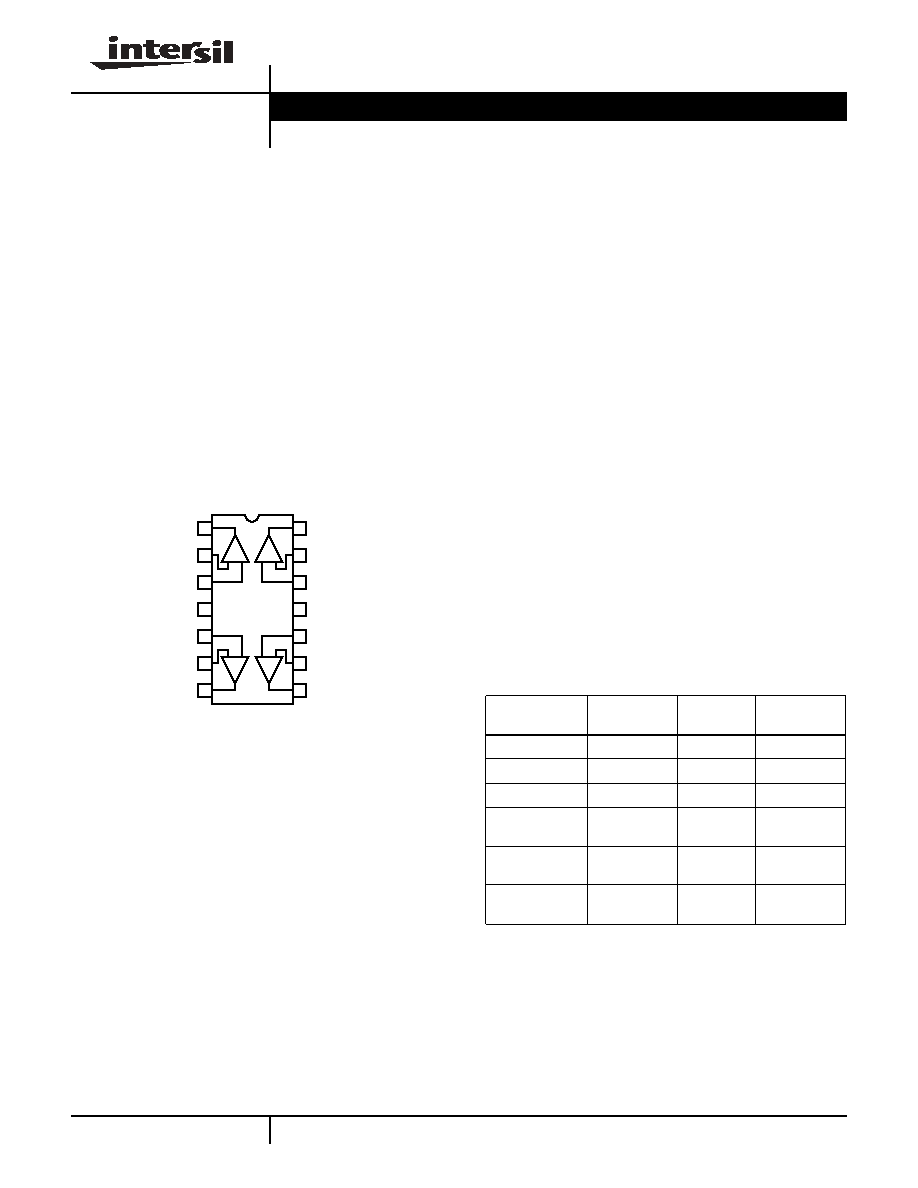
The EL5462 is available in a 14-pin SO package and
operates over the industrial temperature range of -40°C to
+85°C.
Pinout
EL5462
(14-PIN SO)
TOP VIEW
Features
· 500MHz -3dB bandwidth
· 4000V/µs slew rate
· 1.5mA supply current per amplifier
· Single and dual supply operation, from 5V to 12V supply
span
· High speed, 1.4GHz product available (EL5167 &
EL5167)
· High speed, 4mA, 630MHz product available (EL5164 &
EL5165)
· Pb-free available (RoHS compliant)
Applications
· Battery-powered equipment
· Handheld, portable devices
· Video amplifiers
· Cable drivers
· RGB amplifiers
· Test equipment
· Instrumentation
· Current-to-voltage converters
- +
-
+
OUTD
IND-
IND+
VS-
INC+
INC-
1
2
3
4
14
13
12
11
5
6
7
10
9
8 OUTC
OUTA
INA-
INA+
VS+
INB+
INB-
OUTB
- +
-
+
A
D
B
C
Ordering Information
PART NUMBER
PACKAGE
TAPE &
REEL
PKG. DWG. #
EL5462IS
14-Pin SO
-
MDP0027
EL5462IS-T7
14-Pin SO
7"
MDP0027
EL5462IS-T13
14-Pin SO
13"
MDP0027
EL5462ISZ
(See Note)
14-Pin SO
(Pb-Free)
-
MDP0027
EL5462ISZ-T7
(See Note)
14-Pin SO
(Pb-Free)
7"
MDP0027
EL5462ISZ-T13
(See Note)
14-Pin SO
(Pb-Free)
13"
MDP0027
NOTE: Intersil Pb-free products employ special Pb-free material sets;
molding compounds/die attach materials and 100% matte tin plate
termination finish, which are RoHS compliant and compatible with
both SnPb and Pb-free soldering operations. Intersil Pb-free products
are MSL classified at Pb-free peak reflow temperatures that meet or
exceed the Pb-free requirements of IPC/JEDEC J STD-020.
Data Sheet
February 14, 2005
2
FN7492.0
February 14, 2005
Absolute Maximum Ratings
(T
A
= 25°C)
Supply Voltage between V
S
+ and V
S
- . . . . . . . . . . . . . . . . . . . 13.2V
Maximum Continuous Output Current . . . . . . . . . . . . . . . . . . . 50mA
Maximum Voltage between IN+ and IN-, Disabled . . . . . . . . . ±1.5V
Current into IN+, IN-, CE . . . . . . . . . . . . . . . . . . . . . . . . . . . . . ±5mA
Slew Rate from V
S
+ to V
S
- . . . . . . . . . . . . . . . . . . . . . . . . . . . 1V/µs
Pin Voltages. . . . . . . . . . . . . . . . . . . . . . . . .V
S
- - 0.5V to V
S
+ +0.5V
Power Dissipation . . . . . . . . . . . . . . . . . . . . . . . . . . . . . See Curves
Operating Junction Temperature . . . . . . . . . . . . . . . . . . . . . . +125°C
Storage Temperature . . . . . . . . . . . . . . . . . . . . . . . .-65°C to +150°C
Ambient Operating Temperature . . . . . . . . . . . . . . . .-40°C to +85°C
CAUTION: Stresses above those listed in "Absolute Maximum Ratings" may cause permanent damage to the device. This is a stress only rating and operation of the
device at these or any other conditions above those indicated in the operational sections of this specification is not implied.
IMPORTANT NOTE: All parameters having Min/Max specifications are guaranteed. Typical values are for information purposes only. Unless otherwise noted, all tests
are at the specified temperature and are pulsed tests, therefore: T
J
= T
C
= T
A
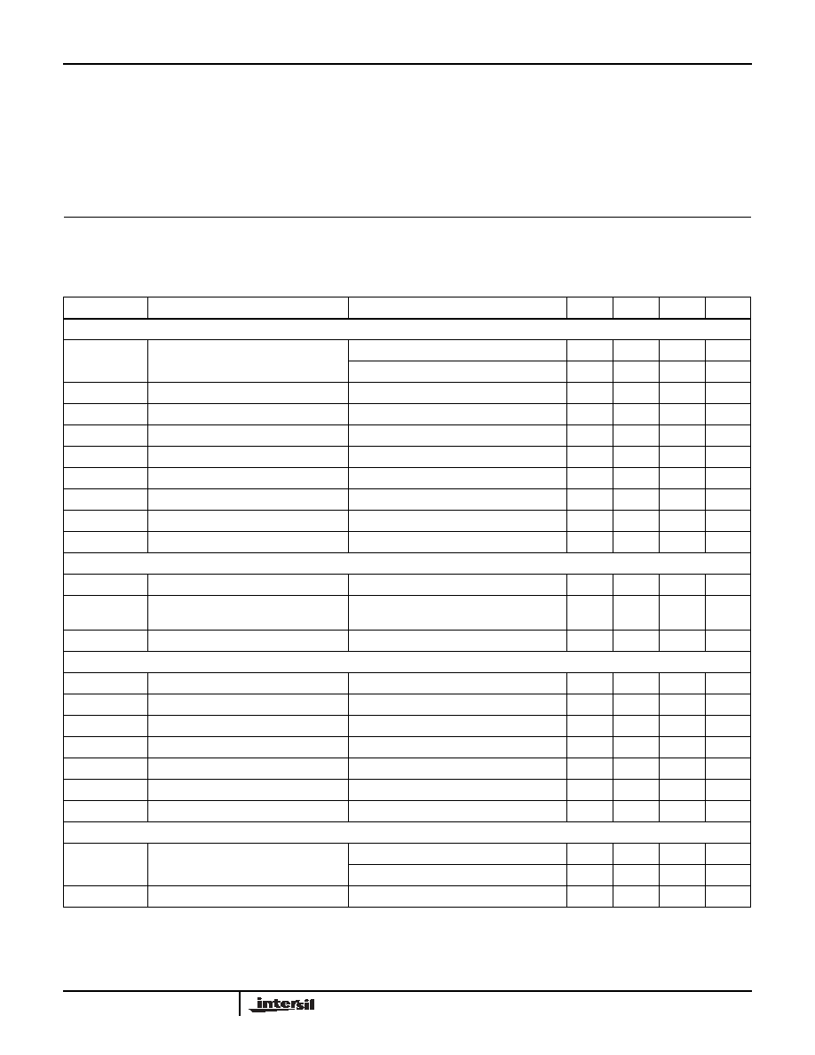
Electrical Specifications
V
S
+
= +5V, V
S
-
= -5V, R
F
= 750
for A
V
= 1, R
F
= 400
for A
V
= 2, R
L
= 150
, T
A
= 25°C unless otherwise
specified.
PARAMETER
DESCRIPTION
CONDITIONS
MIN
TYP
MAX
UNIT
AC PERFORMANCE
BW
-3dB Bandwidth
A
V
= +1, R
L
= 500
, R
F
= 598
500
MHz
A
V
= +2, R
L
= 150
, R
F
= 422
233
MHz
BW1
0.1dB Bandwidth
30
MHz
SR
Slew Rate
V
O
= -2.5V to +2.5V, A
V
= +2, R
L
= 100
2500
4000
5000
V/µs
t
S
0.1% Settling Time
V
OUT
= -2.5V to +2.5V, A
V
= +1
25
ns
e
N
Input Voltage Noise
3
nV/
Hz
i
N
-
IN- Input Current Noise
10
pA/
Hz
i
N
+
IN+ Input Current Noise
6.5
pA/
Hz
dG
Differential Gain Error (Note 1)
A
V
= +2
0.05
%
dP
Differential Phase Error (Note 1)
A
V
= +2
0.15
°
DC PERFORMANCE
V
OS
Offset Voltage
-5
1.5
+5
mV
T
C
V
OS
Input Offset Voltage Temperature
Coefficient
Measured from T
MIN
to T
MAX
6
µV/°C
R
OL
Transimpedance
500
1000
k
INPUT CHARACTERISTICS
CMIR
Common Mode Input Range
Guaranteed by CMRR test
±3
±3.3
V
CMRR
Common Mode Rejection Ratio
V
IN
= ±3V
50
62
75
dB
-ICMR
- Input Current Common Mode Rejection
-1
0.22
+1
µA/V
+I
IN
+ Input Current
-8
0.5
+8
µA
-I
IN
- Input Current
-10
2
+10
µA
R
IN
Input Resistance
0.8
1.6
3
M
C
IN
Input Capacitance
1
pF
OUTPUT CHARACTERISTICS
V
O
Output Voltage Swing
R
L
= 150
to GND
±3.35
±3.6
±3.75
V
R
L
= 1k
to GND
±3.75
±3.9
±4.15
V
I
OUT
Output Current
R
L
= 10
to GND
60
100
mA
EL5462
3
FN7492.0
February 14, 2005
SUPPLY
I
SON
Supply Current - Enabled, per Amplifier
No load, V
IN
= 0V
1.3
1.5
1.7
mA
PSRR
Power Supply Rejection Ratio
DC, V
S
= ±4.75V to ±5.25V
65
76
dB
-IPSR
- Input Current Power Supply Rejection
DC, V
S
= ±4.75V to ±5.25V
-0.5
0.1
+0.5
µA/V
NOTE:
1. Standard NTSC test, AC signal amplitude = 286mV
P-P
, f = 3.58MHz
Electrical Specifications
V
S
+
= +5V, V
S
-
= -5V, R
F
= 750
for A
V
= 1, R
F
= 400
for A
V
= 2, R
L
= 150
, T
A
= 25°C unless otherwise
specified. (Continued)
PARAMETER
DESCRIPTION
CONDITIONS
MIN
TYP
MAX
UNIT
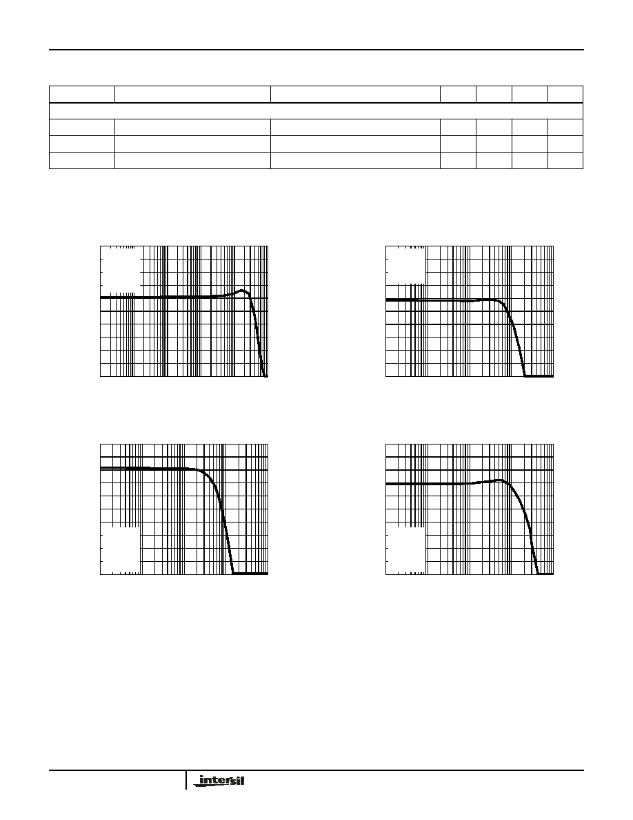
Typical Performance Curves
FIGURE 1. FREQUENCY RESPONSE FOR A
V
=+1
FIGURE 2. FREQUENCY RESPONSE FOR A
V
=+4.6
FIGURE 3. FREQUENCY RESPONSE FOR A
V
=+10
FIGURE 4. FREQUENCY RESPONSE FOR A
V
=+2
NORMALIZ
E
D
GAIN
(dB)
4
10K
100K
1M
10M
100M
1G
2
0
-2
-4
-6
FREQUENCY (Hz)
A
V
=+1
V
CC
=+5V
V
EE
=-5V
R
L
=500
R
F
=598
NORMALIZ
E
D
GAIN
(dB)
4
100K
1M
10M
100M
1G
2
0
-2
-4
-6
FREQUENCY (Hz)
A
V
=+4.6
V
CC
=+5V
V
EE
=-5V
R
F
=375
N
O
RM
AL
IZE
D
G
A
IN
(
d
B)
2
100K
1M
10M
100M
1G
0
-2
-4
-6
-8
FREQUENCY (Hz)
A
V
=+10
V
CC
=+5V
V
EE
=-5V
R
L
=150
R
F
=375
N
O
RM
AL
IZE
D
G
A
IN
(
d
B)
3
100K
1M
10M
100M
1G
1
-1
-3
-5
-7
FREQUENCY (Hz)
A
V
=+2
V
CC
=+5V
V
EE
=-5V
R
L
=150
R
F
=422
EL5462
4
FN7492.0
February 14, 2005
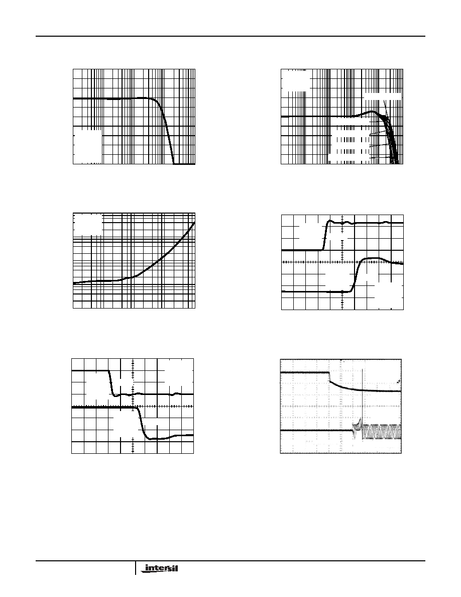
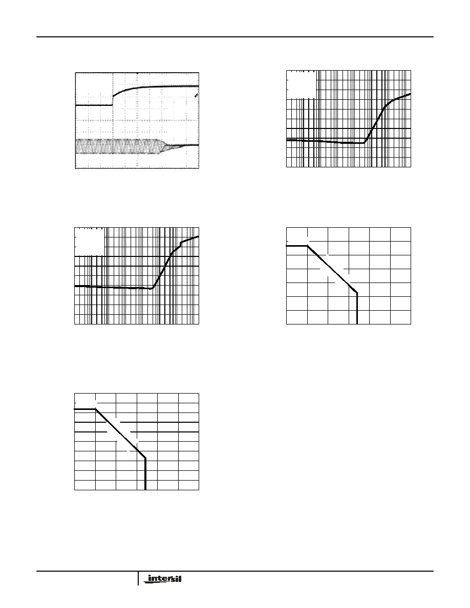
FIGURE 5. FREQUENCY RESPONSE FOR A
V
=+4
FIGURE 6. FREQUENCY RESPONSE FOR VARIOUS V
CC
, V
EE
FIGURE 7. CLOSED LOOP OUTPUT IMPEDANCE
FIGURE 8. OUTPUT RISE TIME
FIGURE 9. OUTPUT FALL TIME
FIGURE 10. TURN ON TIME
Typical Performance Curves
(Continued)
NORMALIZED GAIN
(dB)
3
100K
1M
10M
100M
1G
1
-1
-3
-5
-7
FREQUENCY (Hz)
A
V
=+4
V
CC
=+5V
V
EE
=-5V
R
L
=150
R
F
=422
NORMALIZED GAIN
(dB)
5
100K
1M
10M
100M
1G
3
1
-1
-3
-5
FREQUENCY (Hz)
A
V
=+1
R
L
=150
R
F
=698
V
CC
,V
EE
=±5V
V
CC
,V
EE
=±4V
V
CC
,V
EE
=±3V
V
CC
,V
EE
=±2.5V
V
CC
,V
EE
=±6V
OUT
P
UT
IMPEDANCE (
)
100
10K
100K
1M
10M
100M
10
1
0.1
0.01
FREQUENCY (Hz)
A
V
=+2
V
CC
=+5V
V
EE
=-5V
4ns/DIV
A
V
=+2
V
CC
=+5V
V
EE
=-5V
R
L
=150
1V/DIV
2V/DIV
OUTPUT
RISE
TIME
2.218ns
INPUT
RISE
TIME
1.028ns
4ns/DIV
A
V
=+2
V
CC
=+5V
V
EE
=-5V
R
L
=150
1V/DIV
2V/DIV
OUTPUT
FALL
TIME
2.21ns
INPUT
FALL
TIME
1.036ns
CH1=5V
CH2=200mV
M=100ns
CH1
CH2
100ns/DIV
EL5462
5
FN7492.0
February 14, 2005
FIGURE 11. TURN OFF TIME
FIGURE 12. PSRR (V
CC
)
FIGURE 13. PSRR (V
EE
)
FIGURE 14. PACKAGE POWER DISSIPATION vs AMBIENT
TEMPERATURE
FIGURE 15. PACKAGE POWER DISSIPATION vs AMBIENT
TEMPERATURE
Typical Performance Curves
(Continued)
CH1=5V
CH2=200mV
M=100ns
CH1
CH2
100ns/DIV
P
S
RR (
d
B)
0
10
100
10K
1M
100M
-20
-40
-60
-80
-100
FREQUENCY (Hz)
A
V
=+2
V
CC
=+5V
V
EE
=-5V
R
L
=150
1K
100K
10M
PSRR (dB)
0
10
100
10K
1M
100M
-20
-40
-60
-80
-100
FREQUENCY (Hz)
A
V
=+2
V
CC
=+5V
V
EE
=-5V
R
L
=150
1K
100K
10M
AMBIENT TEMPERATURE (°C)
0
25
50
75 85 100
125
150
POWER DIS
S
IP
A
T
ION
(
W
)
1.4
1
0.6
0.2
0
0.8
0.4
1.2 1.136W
JA
=8
8°C
/W
SO
14
JEDEC JESD51-7 HIGH EFFECTIVE THERMAL
CONDUCTIVITY TEST BOARD
AMBIENT TEMPERATURE (°C)
0
25
50
75 85 100
125
150
P
O
WER DIS
S
IP
A
T
ION
(
W
)
1
0.9
0.6
0.2
0
0.8
0.4
JA
=1
20
°C
/W
SO
14
JEDEC JESD51-3 LOW EFFECTIVE THERMAL
CONDUCTIVITY TEST BOARD
0.5
0.1
0.7
0.3
833mW
EL5462