Äîêóìåíòàöèÿ è îïèñàíèÿ www.docs.chipfind.ru
1
®
FN7507.1
CAUTION: These devices are sensitive to electrostatic discharge; follow proper IC Handling Procedures.
1-888-INTERSIL or 321-724-7143
|
Intersil (and design) is a registered trademark of Intersil Americas Inc.
Copyright © Intersil Americas Inc. 2004, 2005. All Rights Reserved.
All other trademarks mentioned are the property of their respective owners.
EL5623
Multi-Channel Buffer
The EL5623 integrates six channels of gamma buffers into a
single device. The top three gamma channels in each device
are designed to swing to the upper supply rail, with the other
three designed to swing to the lower rail. The output
capability of each channel is 10mA continuous, with 120mA
peak. The gamma buffers feature a 10MHz -3dB bandwidth
specification and a 9V/µs slew rate.
Packaged in the 16-pin TSSOP package, the EL5623 is
specified for operation over the -40°C to +85°C temperature
range.
Features
· Six gamma buffers
- 10MHz BW
- 9V/µs SR
- 120mA peak I
OUT
- 3 high side drivers
- 3 low side drivers
· 3.5mA supply current
· Pb-free available (RoHS compliant)
Applications
· TFT-LCD monitors
· LCD televisions
· Industrial flat panel displays
Pinout
EL5623
(16-PIN TSSOP)
TOP VIEW
Ordering Information
PART NUMBER
(See Note)
PACKAGE
(Pb-Free)
TAPE &
REEL
PKG DWG. #
EL5623IRZ
16-Pin TSSOP
-
MDP0048
EL5623IRZ-T7
16-Pin TSSOP
7"
MDP0048
EL5623IRZ-T13
16-Pin TSSOP
13"
MDP0048
NOTE: Intersil Pb-free products employ special Pb-free material sets;
molding compounds/die attach materials and 100% matte tin plate
termination finish, which are RoHS compliant and compatible with
both SnPb and Pb-free soldering operations. Intersil Pb-free products
are MSL classified at Pb-free peak reflow temperatures that meet or
exceed the Pb-free requirements of IPC/JEDEC J STD-020.
1
2
3
4
12
11
10
9
5
6
7
8
16
15
14
13
VS+
OUT1
OUT2
OUT3
OUT4
OUT5
OUT6
VS-
VS+
IN1
IN2
IN3
IN4
IN5
IN6
VS-
Data Sheet
May 6, 2005
2
FN7507.1
May 6, 2005
NOTE: All parameters having Min/Max specifications are guaranteed. Typ values are for information purposes only. Unless otherwise noted, all tests
are at the specified temperature and are pulsed tests, therefore: T
J
= T
C
= T
A
Absolute Maximum Ratings
(T
A
= 25°C)
Supply Voltage between V
S
+ and V
S
- . . . . . . . . . . . . . . . . . . . .+18V
Input Voltage . . . . . . . . . . . . . . . . . . . . . . . . . . V
S
- -0.5V, V
S
+ +0.5V
Maximum Continuous Output Current (V
OUT1-6
) . . . . . . . . . . 15mA
Power Dissipation . . . . . . . . . . . . . . . . . . . . . . . . . . . . . See Curves
Maximum Die Temperature . . . . . . . . . . . . . . . . . . . . . . . . . . +125°C
Storage Temperature . . . . . . . . . . . . . . . . . . . . . . . .-65°C to +150°C
Ambient Operating Temperature . . . . . . . . . . . . . . . .-40°C to +85°C
CAUTION: Stresses above those listed in "Absolute Maximum Ratings" may cause permanent damage to the device. This is a stress only rating and operation of the
device at these or any other conditions above those indicated in the operational sections of this specification is not implied.
Electrical Specifications
V
S
+ = +15V, V
S
- = 0, R
L
= 10k
, C
L
= 10pF to 0V, and T
A
= 25°C Unless Otherwise Specified
PARAMETER
DESCRIPTION
CONDITIONS
MIN
TYP
MAX
UNIT
INPUT CHARACTERISTICS (REFERENCE BUFFERS)
V
OS
Input Offset Voltage
V
CM
= 0V
2
20
mV
TCV
OS
Average Offset Voltage Drift
(Note 1)
5
µV/
°C
I
B
Input Bias Current
V
CM
= 0V
2
50
nA
R
IN
Input Impedance
10
M
C
IN
Input Capacitance
1.35
pF
A
V
Voltage Gain
1V
V
OUT
14V
0.992
1.008
V/V
CMIR
Input Voltage Range
IN1 to IN3
1.5
V
S
+
V
IN4 to IN6
0
V
S
+
-1.5
V
OUTPUT CHARACTERISTICS (REFERENCE BUFFERS)
V
OH
High Level Output Voltage -
(OUT1)
V
S
+ = 15V, I
O
= 5mA, V
I
= 15V, T
O
= 25°C
14.85
14.9
V
High Level Output Voltage -
(OUT2-OUT3)
14.8
14.85
V
High Level Output Voltage -
(OUT4-OUT6)
V
S
+ = 15V, I
O
= 5mA, V
I
= 13.5V, T
O
= 25°C
13.45
13.5
V
V
OL
Low Level Output Voltage -
(OUT1-OUT3)
V
S
+ = 15V, I
O
= 5mA, V
I
= 1.5V, T
O
= 25°C
1.5
1.55
V
Low Level Output Voltage -
(OUT4-OUT5)
V
S
+ = 15V, I
O
= 5mA, V
I
= 0V, T
O
= 25°C
0.15
.2
V
Low Level Output Voltage -
(OUT6)
0.1
0.15
V
POWER SUPPLY PERFORMANCE
PSRR
Power Supply Rejection Ratio
Reference buffer V
S
from 5V to 15V
50
80
dB
I
S
Total Supply Current
3.5
4.5
mA
DYNAMIC PERFORMANCE (BUFFER AMPLIFIERS)
SR
Slew Rate (Note 2)
5
9
V/µs
t
S
Settling to +0.1% (A
V
= +1)
(A
V
= +1), V
O
= 2V step
500
ns
BW
-3dB Bandwidth
R
L
= 10k
, C
L
= 10pF
10
MHz
GBWP
Gain-Bandwidth Product
R
L
= 10k
, C
L
= 10pF
6
MHz
PM
Phase Margin
R
L
= 10k
, C
L
= 10pF
50
°
CS
Channel Separation
f = 5MHz
75
dB
NOTES:
1. Measured over operating temperature range.
2. Slew rate is measured on rising and falling edges.
EL5623
3
FN7507.1
May 6, 2005
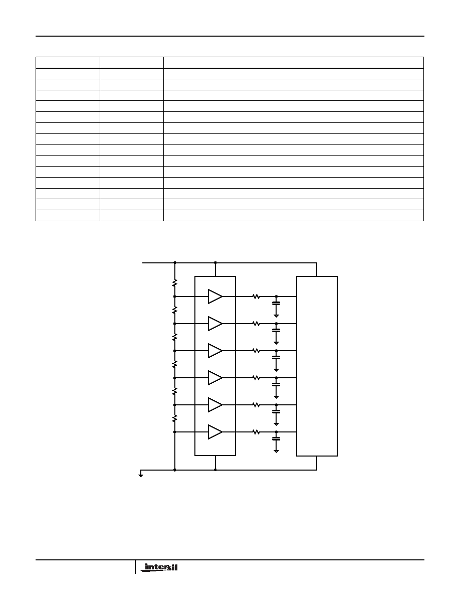
Block Diagram
Pin Descriptions
PIN NUMBER
PIN NAME
PIN FUNCTION
1, 16
VS+
Positive supply voltage
2
OUT1
Output gamma channel 1
3
OUT2
Output gamma channel 2
4
OUT3
Output gamma channel 3
5
OUT4
Output gamma channel 4
6
OUT5
Output gamma channel 5
7
OUT6
Output gamma channel 6
8, 9
VS-
Negative supply
10
IN6
Input gamma channel 6
11
IN5
Input gamma channel 5
12
IN4
Input gamma channel 4
13
IN3
Input gamma channel 3
14
IN2
Input gamma channel 2
15
IN1
Input gamma channel 1
V
S
+
COLUMN
DRIVER
EL5623
EL5623
4
FN7507.1
May 6, 2005
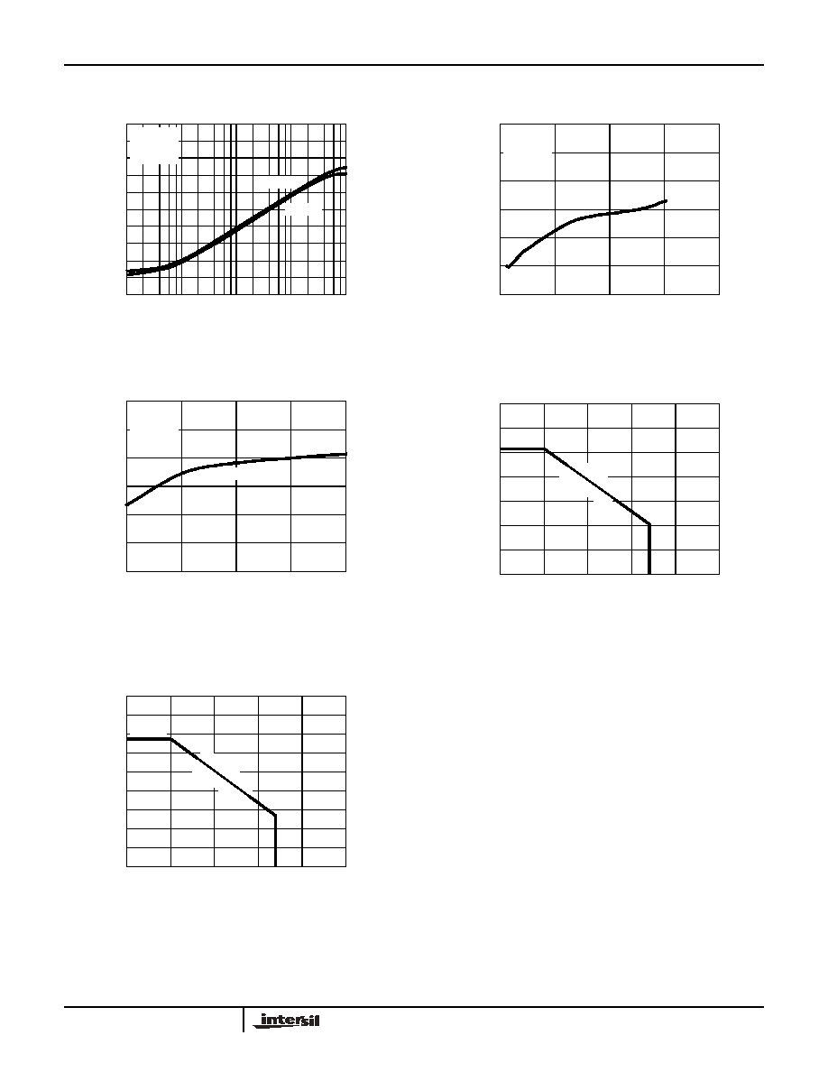
Typical Performance Curves
FIGURE 1. FREQUENCY RESPONSE FOR VARIOUS R
LOAD
FIGURE 2. FREQUENCY RESPONSE FOR VARIOUS C
LOAD
FIGURE 3. LARGE SIGNAL TRANSIENT RESPONSE
FIGURE 4. SMALL SIGNAL TRANSIENT RESPONSE
FIGURE 5. OUTPUT IMPEDANCE vs FREQUENCY
FIGURE 6. INPUT NOISE SPECTRAL DENSITY vs FREQUENCY
100
1K
10K
100K
1M
10M
100M
FREQUENCY (Hz)
GAIN (d
B)
5
3
1
-1
-3
-5
R
L
=150
R
L
=562
R
L
=10k
R
L
=1k
V
S
=±7.5V
C
L
=10pF
1K
10K
100K
1M
10M
100M
1G
FREQUENCY (Hz)
GAIN (d
B)
10
6
2
-2
-6
-10
C
L
=12pF
C
L
=47pF
C
L
=100pF
V
S
=±7.5V
R
L
=10k
V
S
=±7.5V
R
L
=10k
C
L
=8pF
1µs/DIV
2V/DIV
V
IN
V
OUT
V
S
=±7.5V
R
L
=10k
C
L
=8pF
100ns/DIV
50mV/DIV
V
IN
V
OUT
1K
10K
100K
1M
10M
FREQUENCY (Hz)
OUTPUT IMP
E
DANCE (
)
1K
100
10
1
0
BUFFER
V
S
=±5V
10K
100K
1M
10M
100M
FREQUENCY (Hz)
VO
L
T
A
G
E N
O
IS
E (
n
V/
Hz)
100
10
V
S
=±7.5V
EL5623
5
FN7507.1
May 6, 2005
FIGURE 7. PSRR vs FREQUENCY
FIGURE 8. OVERSHOOT vs CAPACITANCE LOAD
FIGURE 9. SETTLING TIME vs STEP SIZE
FIGURE 10. PACKAGE POWER DISSIPATION vs AMBIENT
TEMPERATURE
FIGURE 11. PACKAGE POWER DISSIPATION vs AMBIENT
TEMPERATURE
Typical Performance Curves
PSRR+
V
S
=±7.5V
R
L
=1k
C
L
=1.5pF
PSRR-
1K
10K
100K
1M
10M
FREQUENCY (Hz)
P
S
RR (
d
B)
20
0
-20
-60
-80
-40
V
S
=±7.5V
R
L
=10k
V
OPP
=1V
0
500
1K
1.5K
2K
C
LOAD
(pF)
OV
ERSHOO
T (%
)
60
50
40
10
0
20
30
V
S
=±7.5V
R
L
=10k
C
L
=8pF
BUFFER
2
3
4
5
6
STEP SIZE (+V)
SETTLI
NG TIME
(ns)
800
700
500
300
200
400
600
0
50
75
100
125
AMBIENT TEMPERATURE (°C)
POWE
R DI
SSI
P
A
TI
ON
(W)
1.4
1
0.6
0.2
0
0.4
0.8
25
85
1.2
JEDEC JESD51-7 - HIGH EFFECTIVE THERMAL
CONDUCTIVITY TEST BOARD
1.031W
JA
=97
°C/W
TS
SO
P16
0
50
75
100
125
AMBIENT TEMPERATURE (°C)
POWER DISS
IP
A
T
ION
(W)
0.9
0.7
0.5
0.3
0
0.4
0.6
25
85
0.8
JEDEC JESD51-3 - LOW EFFECTIVE THERMAL
CONDUCTIVITY TEST BOARD
0.2
0.1
676mW
JA
=14
8°C
/W
TSS
OP
16
EL5623