1
®
FN7346.1
EL5524, EL5624, EL5724, EL5824
Integrated Buffers with V
COM
The EL5524, EL5624, EL5724, and EL5824 integrate a
number of gamma reference buffers with a single V
COM
amplifier. The EL5524 contains 4 gamma buffers, the
EL5624 contains 6, the EL5724 contains 8, and the EL5824
contains 10. Each gamma buffer has a bandwidth of 12MHz
and features a slew rate of 15V/µs. The output current is
rated at 30mA continuous, 140mA peak.
The V
COM
amplifiers are rated for 60mA continuous output
current and 200mA peak. They also feature higher slew rate
and bandwidth for use in error cancellation circuits.
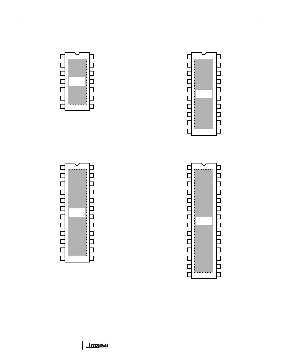
The EL5524 is available in the 14-pin HTSSOP package, the
EL5624 in the 20-pin HTSSOP package, the EL5724 in the
24-pin HTSSOP package, and the EL5824 in the 28-pin
HTSSOP package. All are specified for operation over the
-40°C to +85°C temperature range.
Features
· 4 x gamma buffers (EL5524)
· 6 x gamma buffers (EL5624)
· 8 x gamma buffers (EL5724)
· 10 x gamma buffers (EL5824)
· Single V
COM
amplifier
· 140mA max V
COM
output current
· Low power
- 5.4mA (EL5524)
- 6.8mA (EL5624)
- 8.3mA (EL5724)
- 9.5mA (EL5824)
· Pb-Free plus Anneal available (RoHS compliant)
Applications
· TFT-LCD displays
· Flat panel monitors
· Notebook displays
· LCD-TVs
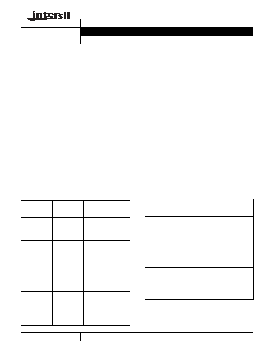
Ordering Information
PART NUMBER
PACKAGE
TAPE &
REEL
PKG. DWG. #
EL5524IRE
14-Pin HTSSOP
-
MDP0048
EL5524IRE-T7
14-Pin HTSSOP
7"
MDP0048
EL5524IRE-T13
14-Pin HTSSOP
13"
MDP0048
EL5524IREZ
(See Note)
14-Pin HTSSOP
(Pb-free)
-
MDP0048
EL5524IREZ-T7
(See Note)
14-Pin HTSSOP
(Pb-free)
7"
MDP0048
EL5524IREZ-T13
(See Note)
14-Pin HTSSOP
(Pb-free)
13"
MDP0048
EL5624IRE
20-Pin HTSSOP
-
MDP0048
EL5624IRE-T7
20-Pin HTSSOP
7"
MDP0048
EL5624IRE-T13
20-Pin HTSSOP
13"
MDP0048
EL5624IREZ
(See Note)
20-Pin HTSSOP
(Pb-free)
-
MDP0048
EL5624IREZ-T7
(See Note)
20-Pin HTSSOP
(Pb-free)
7"
MDP0048
EL5624IREZ-T13
(See Note)
20-Pin HTSSOP
(Pb-free)
13"
MDP0048
EL5724IRE
24-Pin HTSSOP
-
MDP0048
EL5724IRE-T7
24-Pin HTSSOP
7"
MDP0048
EL5724IRE-T13
24-Pin HTSSOP
13"
MDP0048
EL5724IREZ
(See Note)
24-Pin HTSSOP
(Pb-free)
-
MDP0048
EL5724IREZ-T7
(See Note)
24-Pin HTSSOP
(Pb-free)
7"
MDP0048
EL5724IREZ-T13
(See Note)
24-Pin HTSSOP
(Pb-free)
13"
MDP0048
EL5824IRE
28-Pin HTSSOP
-
MDP0048
EL5824IRE-T7
28-Pin HTSSOP
7"
MDP0048
EL5824IRE-T13
28-Pin HTSSOP
13"
MDP0048
EL5824IREZ
(See Note)
28-Pin HTSSOP
(Pb-free)
-
MDP0048
EL5824IREZ-T7
(See Note)
28-Pin HTSSOP
(Pb-free)
7"
MDP0048
EL5824IREZ-T13
(See Note)
28-Pin HTSSOP
(Pb-free)
13"
MDP0048
NOTE: Intersil Pb-free products employ special Pb-free material sets;
molding compounds/die attach materials and 100% matte tin plate
termination finish, which are RoHS compliant and compatible with both
SnPb and Pb-free soldering operations. Intersil Pb-free products are
MSL classified at Pb-free peak reflow temperatures that meet or
exceed the Pb-free requirements of IPC/JEDEC J STD-020.
Ordering Information
(Continued)
PART NUMBER
PACKAGE
TAPE &
REEL
PKG. DWG. #
Data Sheet
May 23, 2005
CAUTION: These devices are sensitive to electrostatic discharge; follow proper IC Handling Procedures.
1-888-INTERSIL or 1-888-352-6832
|
Intersil (and design) is a registered trademark of Intersil Americas Inc.
Copyright Intersil Americas Inc. 2003, 2005. All Rights Reserved
All other trademarks mentioned are the property of their respective owners.
3
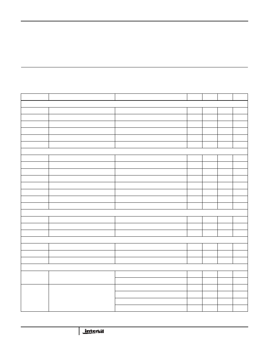
NOTE: All parameters having Min/Max specifications are guaranteed. Typ values are for information purposes only. Unless otherwise noted, all tests
are at the specified temperature and are pulsed tests, therefore: T
J
= T
C
= T
A
Absolute Maximum Ratings
(T
A
= 25°C)
Supply Voltage between V
S
+ and V
S
- . . . . . . . . . . . . . . . . . . . .+18V
Input Voltage . . . . . . . . . . . . . . . . . . . . . . . . . . V
S
- -0.5V, V
S
+ +0.5V
Maximum Continuous Output Current (Buffer) . . . . . . . . . . . . 30mA
Maximum Continuous Output Current (V
COM
) . . . . . . . . . . . . 60mA
Power Dissipation . . . . . . . . . . . . . . . . . . . . . . . . . . . . . See Curves
Maximum Die Temperature . . . . . . . . . . . . . . . . . . . . . . . . . . +125°C
Storage Temperature . . . . . . . . . . . . . . . . . . . . . . . .-65°C to +150°C
Operating Conditions . . . . . . . . . . . . . . . . . . . . . . . . .-40°C to +85°C
CAUTION: Stresses above those listed in "Absolute Maximum Ratings" may cause permanent damage to the device. This is a stress only rating and operation of the
device at these or any other conditions above those indicated in the operational sections of this specification is not implied.
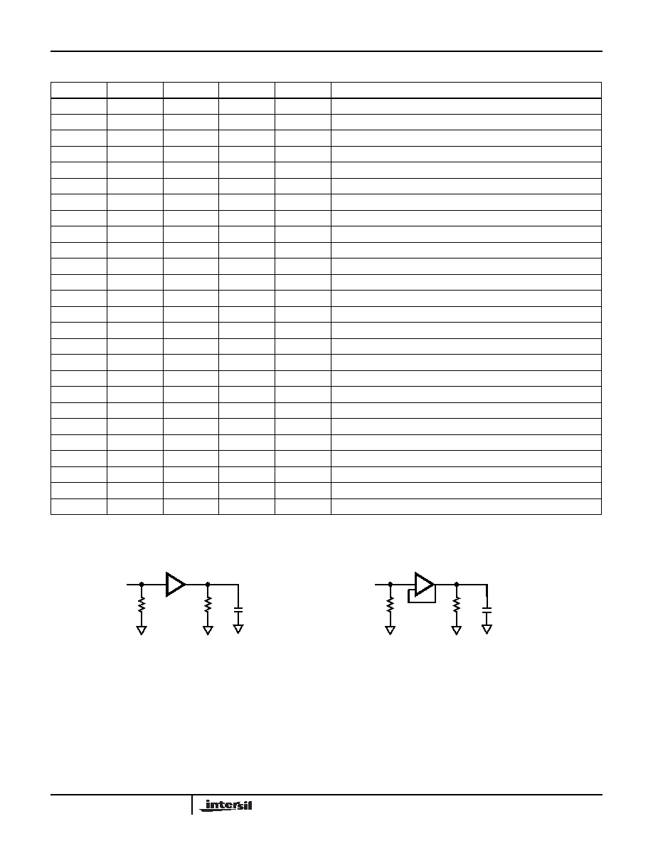
Electrical Specifications
V
S
+ = +15V, V
S
- = 0, R
L
= 10k
, C
L
= 10pF to 0V, Gain of V
COM
= 1, RLV
CM
= 1k
and
T
A
= 25°C Unless Otherwise Specified
PARAMETER
DESCRIPTION
CONDITIONS
MIN
TYP
MAX
UNIT
INPUT CHARACTERISTICS (REFERENCE BUFFERS)
V
OS
Input Offset Voltage
V
CM
= 0V
2
14
mV
TCV
OS
Average Offset Voltage Drift
(Note 1)
5
µV/
°C
I
B
Input Bias Current
V
CM
= 0V
2
50
nA
R
IN
Input Impedance
1
G
C
IN
Input Capacitance
1.35
pF
A
V
Voltage Gain
1V
V
OUT
14V
0.992
1.008
V/V
INPUT CHARACTERISTICS (V
COM
AMPLIFIER)
V
OS
Input Offset Voltage
V
CM
= 7.5V
1
15
mV
TCV
OS
Average Offset Voltage Drift
(Note 1)
5
µV/
°C
I
B
Input Bias Current
V
CM
= 7.5V
2
50
nA
R
IN
Input Impedance
1
G
C
IN
Input Capacitance
1.35
pF
V
REG
Load Regulation
V
COM
= 1.5V, -60mA < I
L
< 60mA
-20
+20
mV
A
VOL
Open Loop Gain
R
L
= 1k
55
75
dB
CMRR
Common Rejection Ratio
45
70
dB
OUTPUT CHARACTERISTICS (REFERENCE BUFFERS)
V
OL
Output Swing Low
I
L
= 7.5mA
50
150
mV
V
OH
Output Swing High
I
L
= 7.5mA
14.85
14.95
V
I
SC
Short Circuit Current
R
L
= 10
±120
±140
mA
OUTPUT CHARACTERISTICS (V
COM
AMPLIFIER)
V
OL
Output Swing Low
I
L
= -7.5mA
50
150
mV
V
OH
Output Swing High
I
L
= +7.5mA
14.85
14.95
V
I
SC
Short Circuit Current
R
L
= 10
±180
±200
mA
POWER SUPPLY PERFORMANCE
PSRR
Power Supply Rejection Ratio
Reference buffer V
S
from 4.5V to 15.5V
55
80
dB
V
COM
buffer, V
S
from 4.5V to 15.5V
55
80
dB
I
S
Total Supply Current
EL5524 (no load)
5.4
7
mA
EL5624 (no load)
6.8
8.5
mA
EL5724 (no load)
8.3
11
mA
EL5824 (no load)
9.5
12.5
mA
EL5524, EL5624, EL5724, EL5824
4
DYNAMIC PERFORMANCE (BUFFER AMPLIFIERS)
SR
Slew Rate (Note 2)
-4V
V
OUT
4V, 20% to 80%
7
15
V/µs
t
S
Settling to +0.1% (A
V
= +1)
(A
V
= +1), V
O
= 2V step
250
ns
BW
-3dB Bandwidth
R
L
= 10k
, C
L
= 10pF
12
MHz
GBWP
Gain-Bandwidth Product
R
L
= 10k
, C
L
= 10pF
8
MHz
PM
Phase Margin
R
L
= 10k
, C
L
= 10pF
50
°
CS
Channel Separation
f = 5MHz
75
dB
DYNAMIC PERFORMANCE (V
COM
AMPLIFIERS)
SR
Slew Rate (Note 2)
-4V
V
OUT
4V, 20% to 80%
65
90
V/µs
t
S
Settling to +0.1% (A
V
= +1)
(A
V
= +1), V
O
= 6V step
150
ns
BW
-3dB Bandwidth
R
L
= 1k
, C
L
= 2pF
35
MHz
GBWP
Gain-Bandwidth Product
R
L
= 1k
, C
L
= 2pF
20
MHz
PM
Phase Margin
R
L
= 1k
, C
L
= 2pF
50
°
NOTES:
1. Measured over operating temperature range
2. Slew rate is measured on rising and falling edges
Electrical Specifications
V
S
+ = +15V, V
S
- = 0, R
L
= 10k
, C
L
= 10pF to 0V, Gain of V
COM
= 1, RLV
CM
= 1k
and
T
A
= 25°C Unless Otherwise Specified
(Continued)
PARAMETER
DESCRIPTION
CONDITIONS
MIN
TYP
MAX
UNIT
EL5524, EL5624, EL5724, EL5824