 | –≠–ª–µ–∫—Ç—Ä–æ–Ω–Ω—ã–π –∫–æ–º–ø–æ–Ω–µ–Ω—Ç: EL5811 | –°–∫–∞—á–∞—Ç—å:  PDF PDF  ZIP ZIP |
1
Æ
FN7355
CAUTION: These devices are sensitive to electrostatic discharge; follow proper IC Handling Procedures.
1-888-INTERSIL or 321-724-7143
|
Intersil (and design) is a registered trademark of Intersil Americas Inc.
Copyright © Intersil Americas Inc. 2004. All Rights Reserved. Elantec is a registered trademark of Elantec Semiconductor, Inc.
All other trademarks mentioned are the property of their respective owners.
EL5611, EL5811
60MHz Rail-to-Rail Input-Output V
COM
Amplifiers
The EL5611 and EL5811 are low
power, high voltage rail-to-rail input-
output amplifiers targeted primarily at
V
COM
applications in TFT-LCD displays. The EL5611
contains six amplifiers, and the EL5811 contains eight
amplifiers. Operating on supplies ranging from 5V to 15V,
while consuming only 2.5mA per amplifier, the EL5611 and
EL5811 have a bandwidth of 60MHz (-3dB). They also
provide common mode input ability beyond the supply rails,
as well as rail-to-rail output capability. This enables these
amplifiers to offer maximum dynamic range at any supply
voltage.
The EL5611 and EL5811 also feature fast slewing and
settling times, as well as a high output drive capability of
65mA (sink and source). In addition to V
COM
applications,
these features make these amplifiers ideal for high speed
filtering and signal conditioning application. Other
applications include battery power, portable devices, and
anywhere low power consumption is important.
The EL5611 is available in 8-pin MSOP and 8-pin HMSOP
packages. The EL5811 is available in space-saving 28-pin
HTSSOP packages.These amplifiers operate over a
temperature range of -40∞C to +85∞C.
Features
∑ 60MHz -3dB bandwidth
∑ Supply voltage = 4.5V to 16.5V
∑ Low supply current (per amplifier) = 2.5mA
∑ High slew rate = 75V/µs
∑ Unity-gain stable
∑ Beyond the rails input capability
∑ Rail-to-rail output swing
∑ ±180mA output short current
∑ Pb-free packaging available
Applications
∑ TFT-LCD panels
∑ V
COM
amplifiers
∑ Drivers for A-to-D converters
∑ Data acquisition
∑ Video processing
∑ Audio processing
∑ Active filters
∑ Test equipment
∑ Battery-powered applications
∑ Portable equipment
Ordering Information
PART NUMBER
PACKAGE
TAPE &
REEL
PKG. DWG. #
EL5611IRE
24-Pin HTSSOP
-
MDP0048
EL5611IRE-T7
24-Pin HTSSOP
7"
MDP0048
EL5611IRE-T13
24-Pin HTSSOP
13"
MDP0048
EL5811IRE
28-Pin HTSSOP
-
MDP0048
EL5811IRE-T7
28-Pin HTSSOP
7"
MDP0048
EL5811IRE-T13
28-Pin HTSSOP
13"
MDP0048
EL5811IREZ
(Note)
28-Pin HTSSOP
(Pb-Free)
-
MDP0048
EL5811IREZ-T7
(Note)
28-Pin HTSSOP
(Pb-Free)
7"
MDP0048
EL5811IREZ-T13
(Note)
28-Pin HTSSOP
(Pb-Free)
13"
MDP0048
NOTE: Intersil Pb-free products employ special Pb-free material
sets; molding compounds/die attach materials and 100% matte tin
plate termination finish, which is compatible with both SnPb and
Pb-free soldering operations. Intersil Pb-free products are MSL
classified at Pb-free peak reflow temperatures that meet or exceed
the Pb-free requirements of IPC/JEDEC J Std-020B.
Data Sheet
May 26, 2004
2
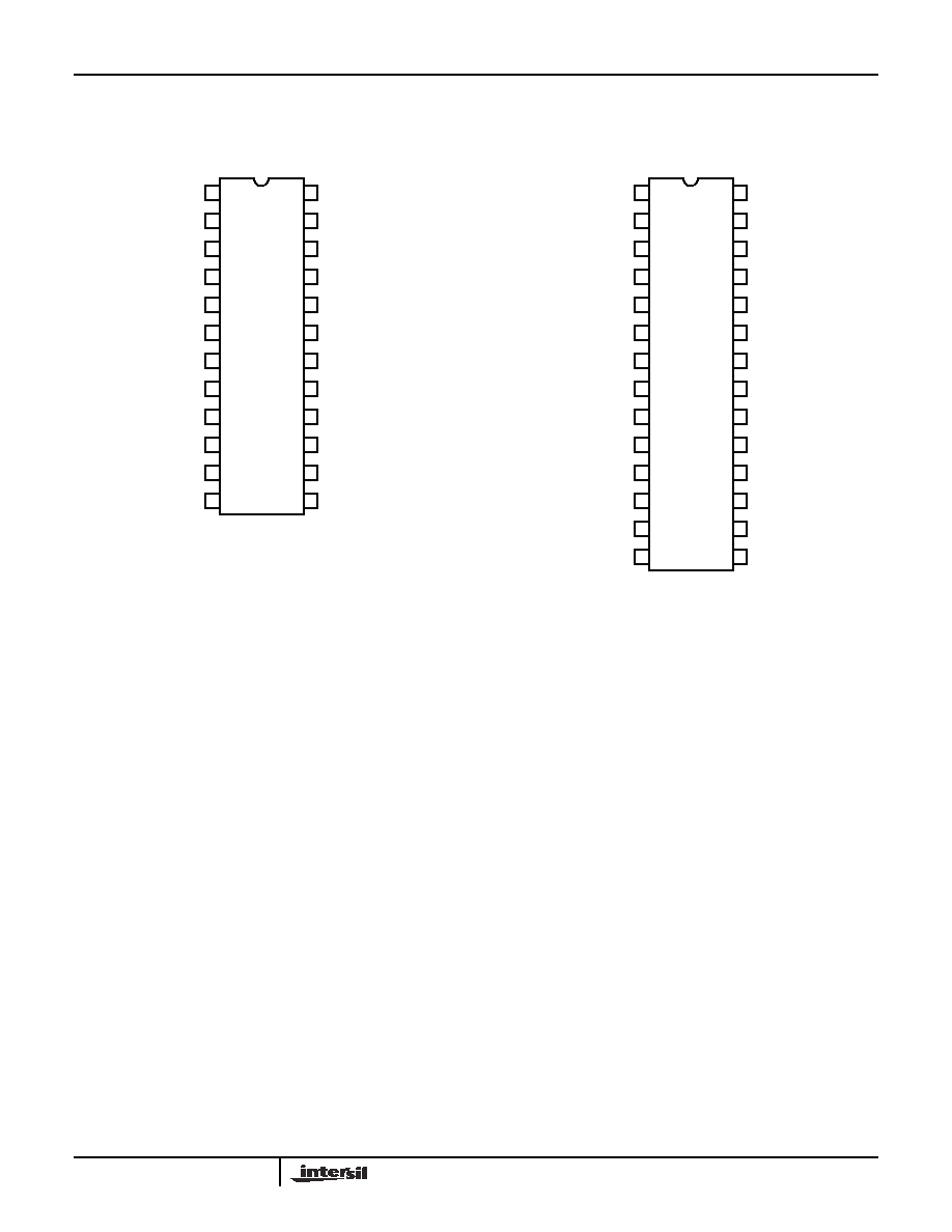
Pinouts
EL5611
(24-PIN HTSSOP)
TOP VIEW
EL5811
(28-PIN HTSSOP)
TOP VIEW
VDD
VOUTF
VINF-
VINF+
VOUTE
VOUTA
VINA-
VINA+
VSS
VOUTB
VINE-
VINE+
VSS
VOUTD+
VINB-
VINB+
VDD
VINC+
VINC-
VOUTD
NC
VOUTC
NC
VOUTD-
1
2
3
4
16
15
14
13
5
6
7
12
11
9
8
10
20
19
18
17
24
23
22
21
VINH+
VINH-
VOUTH
VOUTG
VING-
VDD
VINA+
VINA-
VOUTA
VOUTB
VING+
VSS
VSS
VINF+
VINB-
VINB+
VINC+
VINC-
VOUTC
VOUTF
VOUTE
VINE-
VINE+
VOUTD
VIND-
VIND+
VDD
VINF-
1
2
3
4
28
27
26
25
5
6
7
24
23
22
8
21
9
10
20
19
11
12
13
18
17
16
14
15
EL5611, EL5811
3
Absolute Maximum Ratings
(T
A
= 25∞C)
Supply Voltage between V
S
+ and V
S
- . . . . . . . . . . . . . . . . . . . .+18V
Input Voltage . . . . . . . . . . . . . . . . . . . . . . . . . . V
S
- - 0.5V, V
S
+0.5V
Maximum Continuous Output Current . . . . . . . . . . . . . . . . . . . 65mA
Maximum Die Temperature . . . . . . . . . . . . . . . . . . . . . . . . . . +125∞C
Storage Temperature . . . . . . . . . . . . . . . . . . . . . . . . -65∞C to +150∞C
Ambient Operating Temperature . . . . . . . . . . . . . . . . -40∞C to +85∞C
Power Dissipation . . . . . . . . . . . . . . . . . . . . . . . . . . . . . See Curves
CAUTION: Stresses above those listed in "Absolute Maximum Ratings" may cause permanent damage to the device. This is a stress only rating and operation of the
device at these or any other conditions above those indicated in the operational sections of this specification is not implied.
IMPORTANT NOTE: All parameters having Min/Max specifications are guaranteed. Typical values are for information purposes only. Unless otherwise noted, all tests
are at the specified temperature and are pulsed tests, therefore: T
J
= T
C
= T
A
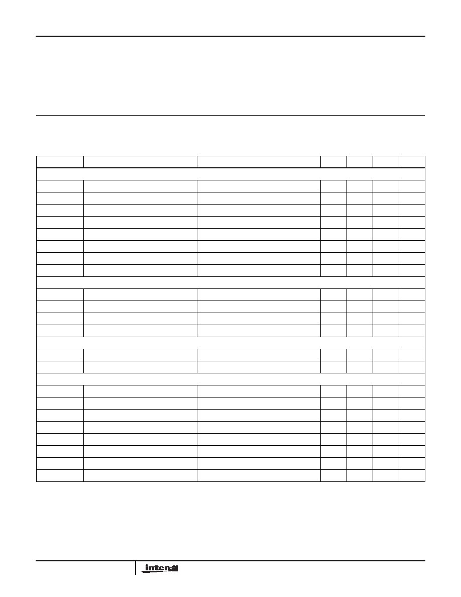
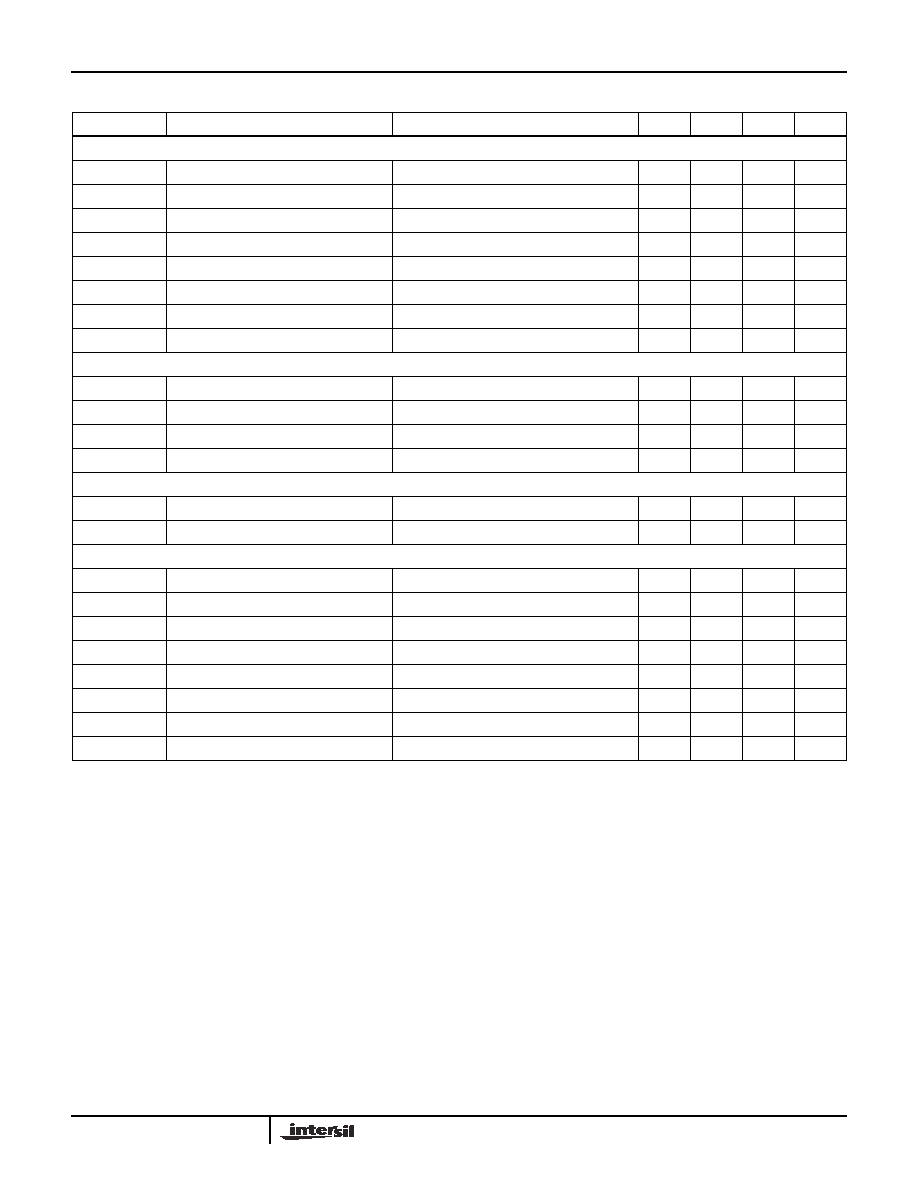
Electrical Specifications
V
S
+ = +5V, V
S
- = -5V, R
L
= 1k
to 0V, T
A
= 25∞C, Unless Otherwise Specified
PARAMETER
DESCRIPTION
CONDITIONS
MIN
TYP
MAX
UNIT
INPUT CHARACTERISTICS
V
OS
Input Offset Voltage
V
CM
= 0V
3
15
mV
TCV
OS
Average Offset Voltage Drift (Note 1)
7
µV/∞C
I
B
Input Bias Current
V
CM
= 0V
2
60
nA
R
IN
Input Impedance
1
G
C
IN
Input Capacitance
2
pF
CMIR
Common-Mode Input Range
-5.5
+5.5
V
CMRR
Common-Mode Rejection Ratio
for V
IN
from -5.5V to 5.5V
50
70
dB
A
VOL
Open-Loop Gain
-4.5V
V
OUT
4.5V
62
70
dB
OUTPUT CHARACTERISTICS
V
OL
Output Swing Low
I
L
= -5mA
-4.92
-4.85
V
V
OH
Output Swing High
I
L
= 5mA
4.85
4.92
V
I
SC
Short-Circuit Current
±180
mA
I
OUT
Output Current
±65
mA
POWER SUPPLY PERFORMANCE
PSRR
Power Supply Rejection Ratio
V
S
is moved from ±2.25V to ±7.75V
60
80
dB
I
S
Supply Current (Per Amplifier)
No load
2.5
3.75
mA
DYNAMIC PERFORMANCE
SR
Slew Rate (Note 2)
-4.0V
V
OUT
4.0V, 20% to 80%
75
V/µs
t
S
Settling to +0.1% (A
V
= +1)
(A
V
= +1), V
O
= 2V step
80
ns
BW
-3dB Bandwidth
60
MHz
GBWP
Gain-Bandwidth Product
32
MHz
PM
Phase Margin
50
∞
CS
Channel Separation
f = 5MHz
110
dB
d
G
Differential Gain (Note 3)
R
F
= R
G
= 1k
and V
OUT
= 1.4V
0.17
%
d
P
Differential Phase (Note 3)
R
F
= R
G
= 1k
and V
OUT
= 1.4V
0.24
∞
NOTES:
1. Measured over operating temperature range.
2. Slew rate is measured on rising and falling edges.
3. NTSC signal generator used.
EL5611, EL5811
4
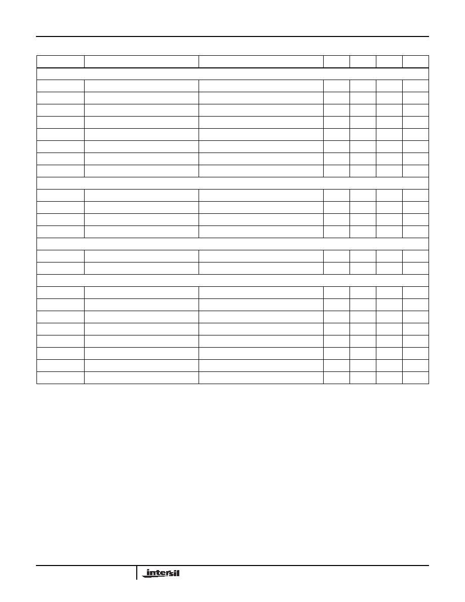
Electrical Specifications
V
S
+ = +5V, V
S
- = 0V, R
L
= 1k
to 2.5V, T
A
= 25∞C, Unless Otherwise Specified
PARAMETER
DESCRIPTION
CONDITION
MIN
TYP
MAX
UNIT
INPUT CHARACTERISTICS
V
OS
Input Offset Voltage
V
CM
= 2.5V
3
15
mV
TCV
OS
Average Offset Voltage Drift (Note 4)
7
µV/∞C
I
B
Input Bias Current
V
CM
= 2.5V
2
60
nA
R
IN
Input Impedance
1
G
C
IN
Input Capacitance
2
pF
CMIR
Common-Mode Input Range
-0.5
+5.5
V
CMRR
Common-Mode Rejection Ratio
for V
IN
from -0.5V to 5.5V
45
66
dB
A
VOL
Open-Loop Gain
0.5V
V
OUT
4.5V
62
70
dB
OUTPUT CHARACTERISTICS
V
OL
Output Swing Low
I
L
= -5mA
80
150
mV
V
OH
Output Swing High
I
L
= 5mA
4.85
4.92
V
I
SC
Short-circuit Current
±180
mA
I
OUT
Output Current
±65
mA
POWER SUPPLY PERFORMANCE
PSRR
Power Supply Rejection Ratio
V
S
is moved from 4.5V to 15.5V
60
80
dB
I
S
Supply Current (Per Amplifier)
No load
2.5
3.75
mA
DYNAMIC PERFORMANCE
SR
Slew Rate (Note 5)
1V
V
OUT
4V, 20% to 80%
75
V/µs
t
S
Settling to +0.1% (A
V
= +1)
(A
V
= +1), V
O
= 2V step
80
ns
BW
-3dB Bandwidth
60
MHz
GBWP
Gain-Bandwidth Product
32
MHz
PM
Phase Margin
50
∞
CS
Channel Separation
f = 5MHz
110
dB
d
G
Differential Gain (Note 6)
R
F
= R
G
= 1k
and V
OUT
= 1.4V
0.17
%
d
P
Differential Phase (Note 6)
R
F
= R
G
= 1k
and V
OUT
= 1.4V
0.24
∞
NOTES:
4. Measured over operating temperature range.
5. Slew rate is measured on rising and falling edges.
6. NTSC signal generator used.
EL5611, EL5811
5
Electrical Specifications
V
S
+ = +15V, V
S
- = 0V, R
L
= 1k
to 7.5V, T
A
= 25∞C, Unless Otherwise Specified
PARAMETER
DESCRIPTION
CONDITION
MIN
TYP
MAX
UNIT
INPUT CHARACTERISTICS
V
OS
Input Offset Voltage
V
CM
= 7.5V
3
15
mV
TCV
OS
Average Offset Voltage Drift (Note 7)
7
µV/∞C
I
B
Input Bias Current
V
CM
= 7.5V
2
60
nA
R
IN
Input Impedance
1
G
C
IN
Input Capacitance
2
pF
CMIR
Common-Mode Input Range
-0.5
+15.5
V
CMRR
Common-Mode Rejection Ratio
for V
IN
from -0.5V to 15.5V
53
72
dB
A
VOL
Open-Loop Gain
0.5V
V
OUT
14.5V
62
70
dB
OUTPUT CHARACTERISTICS
V
OL
Output Swing Low
I
L
= -5mA
80
150
mV
V
OH
Output Swing High
I
L
= 5mA
14.85
14.92
V
I
SC
Short-circuit Current
±180
mA
I
OUT
Output Current
±65
mA
POWER SUPPLY PERFORMANCE
PSRR
Power Supply Rejection Ratio
V
S
is moved from 4.5V to 15.5V
60
80
dB
I
S
Supply Current (Per Amplifier)
No load
2.5
3.75
mA
DYNAMIC PERFORMANCE
SR
Slew Rate (Note 8)
1V
V
OUT
14V, 20% to 80%
75
V/µs
t
S
Settling to +0.1% (A
V
= +1)
(A
V
= +1), V
O
= 2V step
80
ns
BW
-3dB Bandwidth
60
MHz
GBWP
Gain-Bandwidth Product
32
MHz
PM
Phase Margin
50
∞
CS
Channel Separation
f = 5MHz
110
dB
d
G
Differential Gain (Note 9)
R
F
= R
G
= 1k
and V
OUT
= 1.4V
0.16
%
d
P
Differential Phase (Note 9)
R
F
= R
G
= 1k
and V
OUT
= 1.4V
0.22
∞
NOTES:
7. Measured over operating temperature range
8. Slew rate is measured on rising and falling edges
9. NTSC signal generator used
EL5611, EL5811