1
Æ
FN7216.2
CAUTION: These devices are sensitive to electrostatic discharge; follow proper IC Handling Procedures.
1-888-INTERSIL or 321-724-7143
|
Intersil (and design) is a registered trademark of Intersil Americas Inc.
Copyright © Intersil Americas Inc. 2003-2004. All Rights Reserved. Elantec is a registered trademark of Elantec Semiconductor, Inc.
All other trademarks mentioned are the property of their respective owners.
EL6201
Low Power 430MHz HFM Oscillator
w/Disable
The EL6201 is a solid state high performance laser
modulation oscillator with external resistor adjustable
frequency and amplitude. The EL6201 is available in both
the 8-pin MSOP and the 5-pin SOT-23, to enable device
placement close to the laser for reduced EMI.
The oscillator frequency is set by connecting a single
external resistor from the R
FREQ
pin to ground. The
oscillator current output amplitude is set by connecting a
single external resistor from the R
AMP
pin to ground. The
oscillator in the MSOP package also contains a high speed
output disable function using the OE pin. The OE pin can be
driven by a high speed timing signal to control precise laser
modulation during read/write operations. The output current
is disabled when a logical zero `L' is driven to the CE pin.
Supply current is reduced to microamps when CE = LOW.
The EL6201 has internal supply bypass capacitors to reduce
oscillation noise spread through supply connections.
Features
∑ Small SOT-23 and MSOP8 packages
∑ Frequency to 430MHz min
∑ Amplitude to 25mA
P-P
min
∑ Output tristate function (MSOP8)
∑ Power-down function (MSOP8)
∑ Single +3.5V to +5.0V supply
∑ Simple to use - only two external resistors required
∑ Independent resistor setting for frequency and amplitude
∑
Pb-Free Available (RoHS Compliant)
Applications
∑ DVD players
∑ DVD-ROM drives
∑ DVD-RAM drives
∑ CD-RW drives
∑ MO drives
∑ Optical pickup head assembly
∑ Laser diode modulation
∑ Local oscillator
∑ Communications lasers
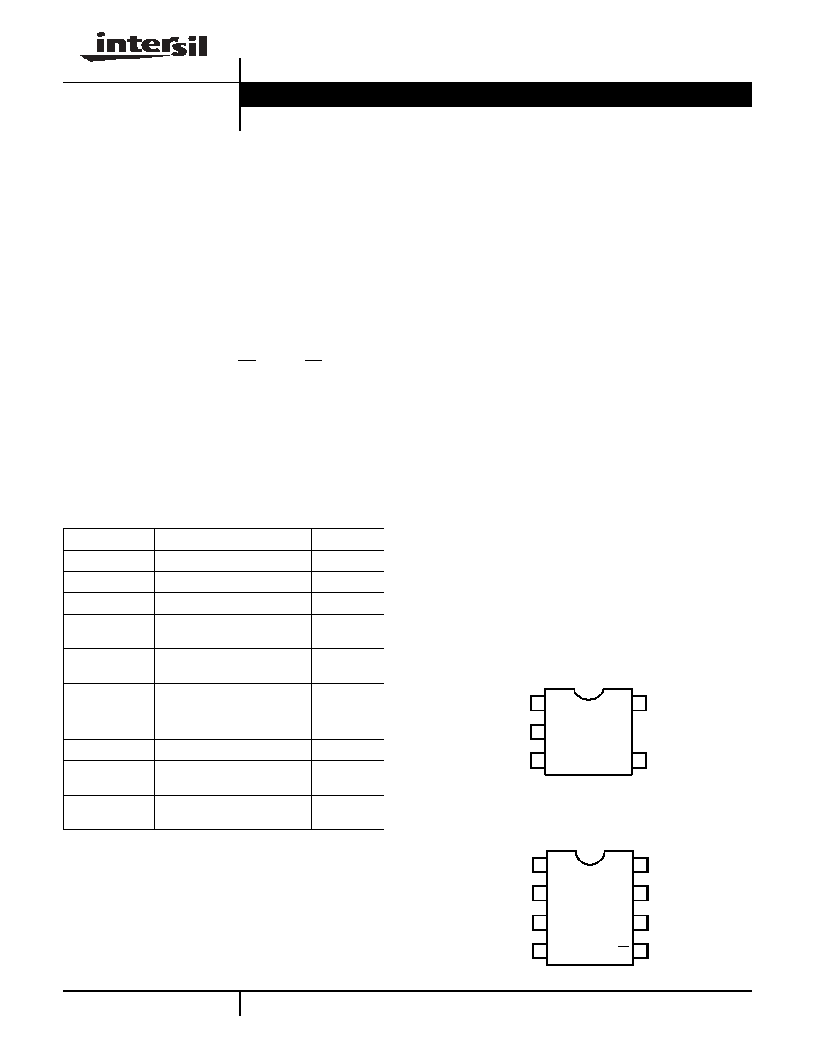
Pinouts
Ordering Information
PART NUMBER
PACKAGE
TAPE & REEL PKG. DWG. #
EL6201CY
8-Pin MSOP
-
MDP0043
EL6201CY-T7
8-Pin MSOP
7" (1.5K pcs)
MDP0043
EL6201CY-T13
8-Pin MSOP
13" (2.5K pcs)
MDP0043
EL6201CYZ
(See Note)
8-Pin MSOP
(Pb-free)
-
MDP0043
EL6201CYZ-T7
(See Note)
8-Pin MSOP
(Pb-free)
7" (1.5K pcs)
MDP0043
EL6201CYZ-T13
(See Note)
8-Pin MSOP
(Pb-free)
13" (2.5K pcs)
MDP0043
EL6201CW-T7
5-Pin SOT-23
7" (3K pcs)
MDP0038
EL6201CW-T7A
5-Pin SOT-23
7" (250 pcs)
MDP0038
EL6201CWZ-T7
(See Note)
5-Pin SOT-23
(Pb-free)
7" (3K pcs)
MDP0038
EL6201CWZ-T7A
(See Note)
5-Pin SOT-23
(Pb-free)
7" (250 pcs)
MDP0038
NOTE: Intersil Pb-free products employ special Pb-free material sets;
molding compounds/die attach materials and 100% matte tin plate
termination finish, which are RoHS compliant and compatible with
both SnPb and Pb-free soldering operations. Intersil Pb-free products
are MSL classified at Pb-free peak reflow temperatures that meet or
exceed the Pb-free requirements of IPC/JEDEC J STD-020C.
1
2
3
4
8
7
6
5
EL6201
(8-PIN MSOP)
TOP VIEW
CE
GND
RFREQ
RAMP
VS
IOUT
GND
OE
1
2
3
5
4
EL6201
(5-PIN SOT-23)
TOP VIEW
VS
GND
IOUT
RFREQ
RAMP
Data Sheet
October 25, 2004

2
Absolute Maximum Ratings
(T
A
= 25∞C)
Voltages applied to:
V
CC . . . . . . . . . . . . . . . . . . . . . . . . . . . . . . . . . . . . . . .
-0.5V to +6.0V
R
FREQ
, R
AMP
. . . . . . . . . . . . . . . . . . . . . . . . . -0.5V to +6.0V
CE, OE . . . . . . . . . . . . . . . . . . . . . . . . . . . . . . . . . 0.5 to V
CC
Power Dissipation (maximum) . . . . . . . . . . . . . . . . . . . . See Curves
Operating Ambient Temperature Range . . . . . . . . . . . 0∞C to +75∞C
Maximum Junction Temperature . . . . . . . . . . . . . . . . . . . . . . . 125∞C
Output Current . . . . . . . . . . . . . . . . . . . . . . . . . . . . . . . . . . . . . 35mA
CAUTION: Stresses above those listed in "Absolute Maximum Ratings" may cause permanent damage to the device. This is a stress only rating and operation of the
device at these or any other conditions above those indicated in the operational sections of this specification is not implied.
IMPORTANT NOTE: All parameters having Min/Max specifications are guaranteed. Typical values are for information purposes only. Unless otherwise noted, all tests
are at the specified temperature and are pulsed tests, therefore: T
J
= T
C
= T
A
DC Electrical Specifications
V
S
= +5V, T
A
= 25∞C, CE = HI, unless otherwise specified. R
AMP
= 6.67k
(I
OUT
= ±8.5mA), R
FREQ
=
833
(F
O
= 330MHz)
PARAMETER
DESCRIPTION
CONDITIONS
MIN
TYP
MAX
UNIT
I
S
Supply Current (Enabled)
CE = HIGH, OE = LOW
20
27
mA
I
SD
Supply Current (Disabled)
CE = LOW
30
µA
I
STRI
Supply Current (Tristated)
OE = HIGH
6.5
8.5
10.5
mA
V
LOAD
Output Voltage Range
Maximum I
OUTP-P
1.5
3.5
V
I
OUTP-P
Output Current Accuracy
R
AMP
= 6.67k, I
OUT
= 2.5V to 3.0V
11
15
19
mA
I
OS
Output Current DC offset
-2.5
0
+2.5
mA
V
INL
Logic Input Low
0.8
V
V
INH
Logic Input High
2.4
V
I
INL
Logic Low Input Current
CE or OE at 0V
100
µA
I
INH
Logic High Input Current
CE or OE at +5V
100
µA
AC Electrical Specifications
V
S
= +5V, T
A
= 25∞C, R
AMP
= 6.67k
, R
FREQ
= 833
PARAMETER
DESCRIPTION
CONDITIONS
MIN
TYP
MAX
UNIT
TC
OSC
Oscillator Temperature Coefficient
Measured from 25∞C to 125∞C die
temperature
600
ppm/∞C
F
OSC
Initial Oscillator Frequency
Accuracy
270
330
400
MHz
F
RANGE
Oscillator Frequency Range
500
R
FREQ
7k
80
430
MHz
A
RANGE
Oscillator Amplitude Range
30k
R
AMP
3k
7.5
25
mA
P-P
T
ON,
CE
EN Delay Time to 50% I
OUT
CE = Low to High
300
ns
T
OFF
, CE
EN Delay Time to 50% I
OUT
CE = High to Low
10
ns
T
ON,
OE
OE Delay Time to 50% I
OUT
OE = Low to High
10
ns
T
OFF
,OE
OE Delay Time to 50% I
OUT
OE = High to Low
10
ns
Duty Cycle
40
52
60
%
EL6201

3
Typical Performance Curves
FIGURE 1. FREQUENCY vs R
FREQ
FIGURE 2. FREQUENCY vs 1000
/R
FREQ
FIGURE 3. I
OUTp-p
vs R
AMP
FIGURE 4. I
OUTp-p
vs 427/R
AMP
FIGURE 5. I
SUPPLY
vs V
SUPPLY
FIGURE 6. DISSIPATION vs SUPPLY VOLTAGE
F
R
EQ
UENCY
(MH
z)
R
FREQ
(k
)
0
1
2
3
5
4
400
300
100
0
200
600
500
I
OUTp-p
= 15mA
T
A
= 25∞C
FREQ
UENCY (
M
Hz)
1000
/R
FREQ
0
3
0
600
1
2
100
200
500
400
300
I
OUTp-p
= 15mA
T
A
= 25∞C
I
OUTp-p
(mA)
R
AMP
(k
)
0
4
8
12
20
16
20
5
0
10
40
35
30
15
25
F
O
= 330MHz
T
A
= 25∞C
I
OUTp-p
(mA)
427/R
AMP
(k
)
0
100
125
150
200
175
20
5
0
10
35
30
15
25
50
75
F
O
= 330MHz
T
A
= 25∞C
ACTUAL
IDEAL
I
S
U
PPL
Y
(mA)
V
SUPPLY
(V)
3.0
3.5
4.0
4.5
5.5
5.0
20
5
0
10
35
30
15
25
F
O
= 330MHz
I
OUTp-p
= 15mA
T
A
= 25∞C
P
DISS
(mW)
V
SUPPLY
(V)
3.0
3.5
4.0
4.5
5.5
5.0
140
80
20
0
40
180
160
120
60
100
F
O
= 330MHz
I
OUTp-p
= 15mA
T
A
= 25∞C
EL6201

4
FIGURE 7. I
OUTP-P
vs V
SUPPLY
FIGURE 8. FREQUENCY vs V
SUPPLY
FIGURE 9. DUTY CYCLE (%) vs V
SUPPLY
FIGURE 10. I
SUPPLY
vs FREQUENCY
FIGURE 11. DISSIPATION vs FREQUENCY
FIGURE 12. I
SUPPLY
vs I
OUTp-p
Typical Performance Curves
(Continued)
I
OUTp-
p
(mA)
V
SUPPLY
(V)
3.0
4.0
5.5
5.0
14
9
8
10
18
17
12
16
13
11
15
3.5
4.5
F
O
= 330MHz
R
AMP
= 6.5k
T
A
= 25∞C
FR
EQ
UENCY (MHz)
V
SUPPLY
(V)
3.0
3.5
4.0
4.5
5.5
5.0
290
260
250
270
320
310
280
300
R
FREQ
= 833
I
OUTp-p
= 15mA
T
A
= 25∞C
DUTY CYC
L
E (%)
V
SUPPLY
(V)
3.0
4.5
5.5
5.0
48.4
47.8
47.6
48.0
48.8
48.2
48.6
3.5
4.0
R
FREQ
= 833
R
AMP
= 6.5k
T
A
= 25∞C
I
SUPPL
Y
(m
A
)
FREQUENCY (MHz)
0
300
500
400
15
10
20
35
30
25
100
200
I
OUTp-p
= 15mA
T
A
= 25∞C
DISSI
P
A
TION (mW
)
FREQUENCY (MHz)
0
100
200
300
500
400
80
60
100
180
140
120
160
I
OUTp-p
= 15mA
V
S
= 5V
T
A
= 25∞C
I
SUPPL
Y
(mA)
I
OUTp-p
(mA)
0
15
25
30
40
35
28
22
20
24
36
34
32
26
30
10
5
20
R
FREQ
= 833
T
A
= 25∞C
EL6201

5
FIGURE 13. DUTY CYCLE vs FREQUENCY
FIGURE 14. OUTPUT SPECTRUM - WIDEBAND
FIGURE 15. I
SUPPLY
vs DIE TEMPERATURE
FIGURE 16. I
OUTp-p
vs DIE TEMPERATURE
FIGURE 17. DUTY CYCLE vs DIE TEMPERATURE
FIGURE 18. FREQUENCY vs DIE TEMPERATURE
Typical Performance Curves
(Continued)
DUTY C
Y
CL
E
(%)
FREQUENCY (MHz)
0
300
500
400
42
40
46
58
56
50
100
200
54
44
48
52
I
OUTp-p
= 15mA
V
S
= 5V
T
A
= 25∞C
RELA
TIVE AMPLITUDE (dB)
FREQUENCY (MHz)
340
355
365
360
-100
-80
0
-50
345
350
-90
-70
-10
-20
-40
-60
-30
R
FREQ
= 833
R
AMP
= 6.5k
T
A
= 25∞C
I
SU
PPL
Y
(mA)
DIE TEMPERATURE (∞C)
0
25
50
75
125
100
26.0
24.5
24.0
25.0
28.0
27.5
27.0
25.5
26.5
F
O
= 330MHz
I
OUTp-p
= 15mA
I
OUTp-p
(m
A)
DIE TEMPERATURE (∞C)
0
25
50
75
125
100
18.5
18.0
19.0
20.5
20.0
19.5
R
FREQ
= 833
R
AMP
= 6.5k
DUTY CYCLE
(
%
)
DIE TEMPERATURE (∞C)
0
25
50
75
125
100
46.0
45.5
46.5
48.5
47.5
47.0
48.0
R
FREQ
= 833
R
AMP
= 6.5k
FREQ
UENC
Y (M
Hz)
DIE TEMPERATURE (∞C)
0
25
125
100
355
340
335
345
380
375
370
350
360
365
50
75
R
FREQ
= 833
R
AMP
= 6.5k
EL6201

6
Typical Application Circuit
Applications Information
The EL6201 is designed to interface easily to laser diodes to
break up optical feedback resonant modes and thereby
reduce laser noise, but it is also generally useful as a 70MHz
- 430MHz oscillator. The first applications section will focus
on laser systems, and subsequent sections are of general
topics.
Laser Diode Applications
The output of the EL6201 is composed of a sourcing and a
sinking current source, switched alternately at the oscillator
frequency. The output voltage compliance is V
S
to ground,
with about 40
of series resistance. There is no severe
squarewave distortion when the output voltage approaches
the supply extremes, although the corners will be rounded.
Being a current-source output, the output bias voltage is set
by direct connection to the laser diode, which will appear as
a low AC impedance with a DC voltage from 1.6V to 2.5V.
Thus AC coupling from the EL6201 to the diode is
unnecessary. The duty cycle of the output is between 40%
and 60%, so the DC contribution from the EL6201 is only
±5% of the peak-to-peak output. This will cause little
perturbation of the diode's DC bias current.
Although not necessary, capacitance coupling can be
employed. A series capacitive reactance of less than 30
is
recommended. A 20pF capacitor is thus appropriate at
330MHz. Benefits include no DC error current into the laser
diode, and an attenuation of low-frequency noise from the
EL6201. Disadvantages include perhaps 20% output AC
current loss.
While the diode AC impedance is generally in the low ohm
range, any interconnect will create around 8nH per cm. of
series inductance. Because the EL6201's output is an AC
current source, higher load reactance due to series
inductance will cause the EL6201's output voltage to swing
more than what a direct connection to the diode would
cause. At 400MHz and 15mA
P-P
output, just one cm. will
generate 0.3V
P-P
of extra driver signal at the fundamental,
and more at harmonic frequencies. The output current
FIGURE 19.
SOT23-5
POWER DISSIPATION vs AMBIENT
TEMPERATURE
FIGURE 20. MSOP8 POWER DISSIPATION vs AMBIENT
TEMPERATURE
Typical Performance Curves
(Continued)
SEMI G42-88 SINGLE LAYER TEST BOARD
PO
W
E
R DI
SSIP
A
ION (
W
)
AMBIENT TEMPERATURE (∞C)
0
25
50
75
125
100
0.10
0.00
0.20
0.50
0.40
0.30
JA
= 256∞C/W
391mW
195mW
SEMI G42-88 SINGLE LAYER TEST BOARD
PO
W
E
R DI
SSIP
A
ION (
W
)
AMBIENT TEMPERATURE (∞C)
0
25
50
75
125
100
0.10
0.00
0.20
0.60
0.50
0.30
JA
= 206∞C/W
486 mW
0.40
243mW
1
2
3
5
4
+5V
+5V
C*
I
DC
R
FREQ
R
AMP
*Optional AC coupling
EL6201

7
waveform is a squarewave, and inductive loads can cause as
much as 1V of overshoot. This does not mean that the
current delivered to the diode has overshoot - just the
voltage seen at the EL6201 output. Measurements show that
the EL6201 output edge rate is about 300psec - a speed
nearly impossible to deliver over practical interconnects to
the diode.
General Considerations
EMI and Grounding
From an EMI point of view, the edge rate of the output
current is much more important than that of the output
voltage. The components are generally small and will be
placed over a ground plane, so antenna effects that launch
voltage-mode EMI are small. Measurement shows that a
practical current edge rate is about 1nsec., so interconnect
should be over a ground plane and short to minimize
inductively launched EMI. Most EMI seems to come from the
supply wires connected to the diode/EL6201 board. The
internal resistance and inductance of capacitors prevents
perfect bypass action, and 150mV
P-P
noise on the lines is
common. There needs to be a lossy series inductance and
secondary bypass on the supply side to control signals from
propagating down the wires. Alternatively, a series supply
resistor can be used, which will also be useful in reducing
EL6201 power dissipation. Figure 22 shows the typical
connection.
The L Series of Figure 22 must be carefully chosen. The
goal is to get a series reactance of around 70
at 300MHz,
so 40nH would suffice. The inductor should be shielded to
reduce EMI and have no saturation effects at the supply
currents drawn by the EL6201. Finally, there should be no
self-resonance at the operating frequency or its harmonics.
Also important is circuit-board layout. At the EL6201's
operating frequencies, even the ground plane is not low-
impedance, and ground loops should be avoided. Figure 23
shows the output current loops:
For the sourcing current loop, the current flows through the
supply bypass capacitor. The ground end of the bypass thus
should be connected directly to the EL6201 ground pin
(output ground pin of the 8-pin package). A long ground
return path will cause the bypass capacitor currents to
generate voltage drops in the ground plane of the circuit
board, and other components (such as R
AMP
and R
FREQ
)
will pick this up as an interfering signal. Similarly, the ground
return of the load should be considered as noisy and other
grounded components should not connect to this path.
Slotting the ground plane around the load's return will
eliminate adjacent grounded components from seeing the
noise.
R
FREQ
and R
AMP
Interfaces
R
AMP
and R
FREQ
should be connected to the non-load side
of the power ground to avoid noise pick-up.
Figure 24 shows an equivalent circuit of these pins. V
REF
is
roughly 0.35V for R
FREQ
and more accurately 1.17V for
R
AMP
. The R
AMP
and R
FREQ
resistor should return to the
EL6201's ground very directly lest they pick up high-
frequency noise interference. They also should have minimal
capacitance to ground. Trimmer resistors can be used to
FIGURE 21. OUTPUT CURRENT WAVEFORM - 1GHz
BANDWIDTH
+5V
V
S
L Series: 70
reactance at
300MHz (see text)
0.1µF
Chip
EL6201
GND
0.1µF
Chip
FIGURE 22. RECOMMENDED SUPPLY BYPASSING
SINKING CURRENT LOOP
SOURCING CURRENT LOOP
SUPPLY
BYPASS
LOAD
R
FREQ
R
AMP
GND
(8-PIN
PACKAGE)
FIGURE 23. OUTPUT CURRENT LOOPS
EL6201

8
All Intersil U.S. products are manufactured, assembled and tested utilizing ISO9000 quality systems.
Intersil Corporation's quality certifications can be viewed at www.intersil.com/design/quality
Intersil products are sold by description only. Intersil Corporation reserves the right to make changes in circuit design, software and/or specifications at any time without
notice. Accordingly, the reader is cautioned to verify that data sheets are current before placing orders. Information furnished by Intersil is believed to be accurate and
reliable. However, no responsibility is assumed by Intersil or its subsidiaries for its use; nor for any infringements of patents or other rights of third parties which may result
from its use. No license is granted by implication or otherwise under any patent or patent rights of Intersil or its subsidiaries.
For information regarding Intersil Corporation and its products, see www.intersil.com
adjust initial operating points, but they should be replaced
with fixed resistors for further testing.
External voltage sources can be coupled to the R
AMP
and
R
FREQ
pins to effect frequency or amplitude modulation or
adjustment. It is recommended that a coupling resistor be
installed in series with the control voltage and mounted
directly next to the EL6201 pin. This will keep the inevitable
high-frequency noise of the EL6201's local environment from
propagating to the modulation source, and it will keep
parasitic capacitance at the EL6201 pin minimized.
Both inputs have several megahertz of bandwidth for analog
modulation. The output enable pin can be used to pass
digital modulation up to about 20Mbit/sec rates.
Power Dissipation Considerations
Supply current can be predicted by the equation:
The 12mA quantity represents the operating DC current of
the EL6201. This is also the current drawn from the supply
during output disable. The I
OUT
quantity is based on a
typical 50% duty cycle of output pull-up current, and the fact
that the peak-to-peak output current is about twice the pull-
up or pull-down currents. The V
S
quantity is due to CV
2
F
losses within the circuit, and the 8*10
-12
quantity represents
internal capacitances that must be slewed at the operating
frequency. The 1.6V offset is a curve fit to measured data.
The internal die temperature operating range is -40∞C to
+125∞C. Internal temperature is equal to the ambient
temperature plus power dissipated times the thermal
resistance of the mounted package,
JA
. For a mounted
MSOP-8 package,
JA
is 206∞C/W. The SOT-23 package
has a
JA
of 256∞C/W.
Power-Down with the SOT-23 Package
The supply current of the EL6201 is low enough so that a
logic output can simply provide the supply current of the part
and effect power-down. This is most useful using the EL6201
in the SOT-23 package, which has no enable pin.
RF Applications
The EL6201 can easily interface to reactive loads, and is
adequate as a short-range modulated transmitter.
Remembering that the output circuitry looks like current
sources, impedance matching becomes a matter of
transforming the load impedance to an appropriate load line
for the EL6201. Also important is maintaining correct DC
bias voltage on the output. Since the output will have a net
DC current, capacitor coupling would allow the DC level to
drift toward a supply rail and increase output harmonic
products. In cases where such harmonics are important,
Figure 25 shows coupling the EL6201 output to a 50
load:
Digital Clock Applications
The EL6201 can be used as a digital clock source. If
unloaded, the output will simply traverse ground to V
S
. It is
recommended that the V
S
supply be isolated from the main
digital supply with an inductor or resistor, whose value is
chosen to drop about 250mV. In this way logic noise can be
isolated by the series component and the EL6201 local
bypass.
The rise- and fall-time of the output will be equal to
V
S
/(C
LOAD
*I
OUTp-p
/2). The output current should be the
smallest that can set an output rise-time, in the interest of
lowest dissipation.
The jitter is about 0.7% of period, RMS.
-
+
PIN
V
REF
FIGURE 24. R
FREQ
AND R
AMP
PIN INTERFACE
I
S
12mA
I
OUTp-p
+
4
V
S
(
- 1.6V
)
FREQ
8
10
-12
◊
◊
◊
+
-------------------------------------------------------------------------------------------------
=
I
OUT
EL6201
L
CHOKE
C1
C2
R1
V
S
R2
L
0.001µF
50
LOAD
FIGURE 25. TUNED INTERFACE TO 50
LEAD
EL6201