
1
Æ
FN7218.2
CAUTION: These devices are sensitive to electrostatic discharge; follow proper IC Handling Procedures.
1-888-INTERSIL or 321-724-7143
|
Intersil (and design) is a registered trademark of Intersil Americas Inc.
Copyright © Intersil Americas Inc. 2003-2004. All Rights Reserved. Elantec is a registered trademark of Elantec Semiconductor, Inc.
All other trademarks mentioned are the property of their respective owners.
EL6203
Laser Driver Oscillator
The EL6203 is a push-pull oscillator used to reduce laser
noise. It uses the standard interface to existing ROM
controllers. The frequency and amplitude are each set with a
separate resistor connected to ground. The tiny package
and harmonic reduction allow the part to be placed close to a
laser with low RF emissions. An auto turn-off feature allows
it to easily be used on combo CD-RW plus DVD-ROM pick-
ups.
One external resistor sets the oscillator frequency. Another
external resistor sets the oscillator amplitude. If the APC
current is reduced such that the average laser voltage drops
to less than 1.1V, the output and oscillator are disabled,
reducing power consumption to a minimum.
The current drawn by the oscillator consists of a small bias
current, plus the peak output amplitude in the positive cycle.
In the negative cycle the oscillator subtracts peak output
amplitude from the laser APC current.
This part is pin-compatible to the EL6201. It is superior to the
EL6201 in several ways: It has up to 100mA output
capability, it is more power-efficient, it has less harmonic
content, and it has an auto shut-off feature activated at 1.1V.
The part is available in the space-saving 5-pin SOT-23
package. It is specified for operation from 0
∞
C to +70
∞
C.
Pinout
EL6203
(5-PIN SOT-23)
TOP VIEW
Features
∑ Low power dissipation
∑ User-selectable frequency from 60MHz to 600MHz
controlled with a single resistor
∑ User-specified amplitude from 10mA
PK-PK
to 100mA
PK
controlled with a single resistor
∑ Auto turn-off threshold
∑ Soft edges for reduced EMI
∑ Small 5-pin SOT-23 package
∑
Pb-free available as an option
Applications
∑ DVD players
∑ DVD-ROM drives
∑ CD-RW drives
∑ MO drives
∑ General purpose laser noise reduction
1
2
3
5
4
VDD
RFREQ
GND
IOUT
RAMP
Ordering Information
PART NUMBER
PACKAGE
TAPE & REEL PKG. DWG. #
EL6203CW-T7
5-Pin SOT-23
7" (3K pcs)
MDP0038
EL6203CW-T7A
5-Pin SOT-23
7" (250 pcs)
MDP0038
EL6203CWZ-T7
(See Note)
5-Pin SOT-23
(Pb-free)
7" (3K pcs)
MDP0038
EL6203CWZ-T7A
(See Note)
5-Pin SOT-23
(Pb-free)
7" (250 pcs)
MDP0038
NOTE: Intersil Pb-free products employ special Pb-free material
sets; molding compounds/die attach materials and 100% matte tin
plate termination finish, which is compatible with both SnPb and
Pb-free soldering operations. Intersil Pb-free products are MSL
classified at Pb-free peak reflow temperatures that meet or exceed
the Pb-free requirements of IPC/JEDEC J STD-020C.
Data Sheet
October 4, 2004

2
Absolute Maximum Ratings
(T
A
= 25∞C)
Voltages Applied to:
V
DD
. . . . . . . . . . . . . . . . . . . . . . . . . . . . . . . . . -0.5V to +6.0V
I
OUT
. . . . . . . . . . . . . . . . . . . . . . . . . . . . . . . . -0.5V to +6.0V
R
FREQ
, R
AMP
. . . . . . . . . . . . . . . . . . . . . . . . . -0.5V to +6.0V
Operating Ambient Temperature Range . . . . . . . . . . . 0∞C to +70∞C
Maximum Junction Temperature . . . . . . . . . . . . . . . . . . . . . . +150∞C
Storage Temperature Range . . . . . . . . . . . . . . . . . .-65∞C to +150∞C
Output Current . . . . . . . . . . . . . . . . . . . . . . . . . . . . . . . 100mA
PK-PK
Power Dissipation (max) . . . . . . . . . . . . . . . . . . . . . . . . See Curves
CAUTION: Stresses above those listed in "Absolute Maximum Ratings" may cause permanent damage to the device. This is a stress only rating and operation of the
device at these or any other conditions above those indicated in the operational sections of this specification is not implied.
IMPORTANT NOTE: All parameters having Min/Max specifications are guaranteed. Typical values are for information purposes only. Unless otherwise noted, all tests
are at the specified temperature and are pulsed tests, therefore: T
J
= T
C
= T
A
Supply & Reference Voltage Characteristics
V
DD
= +5V, T
A
= 25∞C, R
L
= 10
, R
FREQ
= 5210
(F
OSC
= 350MHz), R
AMP
=
2540
(I
OUT
= 50mA
P-P
measured at 60MHz), V
OUT
= 2.2V
PARAMETER
DESCRIPTION
CONDITIONS
MIN
TYP
MAX
UNIT
PSOR
Power Supply Operating Range
4.5
5.5
V
I
SO
Supply Current Disabled
V
OUT
< V
CUTOFF
550
750
µA
I
STYP
Supply Current Typical Conditions
R
FREQ
= 5.21k
,
R
AMP
= 2.54k
18.5
22
mA
I
SLO
Supply Current Low Conditions
R
FREQ
= 30.5k
, R
AMP
= 12.7k
4.75
mA
I
SHI
Supply Current High Conditions
R
FREQ
= 3.05k
,
R
AMP
= 1.27k
32
mA
V
FREQ
Voltage at R
FREQ
Pin
1.27
V
V
RAMP
Voltage on RAMP Pin
1.27
V
V
CUTOFF
Monitoring Voltage of I
OUT
Pin
1.1
1.4
V
Oscillator Characteristics
V
DD
= +5V, T
A
= 25∞C, R
L
= 10
, R
FREQ
= 5210
(F
OSC
= 350MHz), R
AMP
= 2540
(I
OUT
= 50mA
P-P
measured at 60MHz), V
OUT
= 2.2V
PARAMETER
DESCRIPTION
CONDITIONS
MIN
TYP
MAX
UNIT
F
OSC
Frequency Tolerance
Unit-unit frequency variation
300
350
400
MHz
F
HIGH
Frequency Range High
R
FREQ
= 3.05k
600
MHz
F
LOW
Frequency Range Low
R
FREQ
= 30.5k
60
MHz
TC
OSC
Frequency Temperature Sensitivity
0∞C to +70∞C ambient
50
ppm/∞C
PSRR
OSC
Frequency Change
F/F
V
DD
from 4.5V to 5.5V
1
%
Driver Characteristics
V
DD
= +5V, T
A
= 25∞C, R
L
= 10
, R
FREQ
= 30.5k
(F
OSC
= 60MHz), R
AMP
= 2540
(I
OUT
= 50mA
P-P
measured at 60MHz), V
OUT
= 2.2V
PARAMETER
DESCRIPTION
CONDITIONS
MIN
TYP
MAX
UNIT
AMP
HIGH
Amplitude Range High
R
AMP
= 1.27k
100
mA
P-P
AMP
LOW
Amplitude Range Low
R
AMP
= 12.7k
10
mA
P-P
IOS
NOM
Offset Current @ 2.2V
R
FREQ
= 5210
,
V
OUT
= 2.2V
-4
mA
IOS
HIGH
Offset Current @ 2.8V
R
FREQ
= 5210
,
V
OUT
= 2.8V
-4.8
mA
IOS
LOW
Offset Current @ 1.8V
R
FREQ
= 5210
,
V
OUT
= 1.8V
-3.5
mA
I
OUTP-P
Output Current Tolerance
Defined as one standard deviation
2
%
Duty Cycle
Output Push Time/Cycle Time
R
FREQ
= 5210
43
%
PSRR
AMP
Amplitude Change of Output
I/I
V
DD
from 4.5V to 5.5V
-54
dB
T
ON
Auto Turn-on Time
Output voltage step from 0V to 2.2V
15
µs
T
OFF
Auto Turn-off Time
Output voltage step from 2.2V to 0V
0.5
µs
IOUT
N
Output Current Noise Density
R
FREQ
= 5210
,
measured @ 10MHz
2.5
nA/
Hz
EL6203

3
Recommended Operating Conditions
V
DD
. . . . . . . . . . . . . . . . . . . . . . . . . . . . . . . . . . . . . . . . . . 5V ±10%
V
OUT
. . . . . . . . . . . . . . . . . . . . . . . . . . . . . . . . . . . . . . . . . . . 2V - 3V
R
FREQ
. . . . . . . . . . . . . . . . . . . . . . . . . . . . . . . . . . . . . . . . 3k
(min)
R
AMP
. . . . . . . . . . . . . . . . . . . . . . . . . . . . . . . . . . . . . . 1.25k
(min)
F
OSC
. . . . . . . . . . . . . . . . . . . . . . . . . . . . . . . . . . . . . . . .60-600MHz
I
OUT
. . . . . . . . . . . . . . . . . . . . . . . . . . . . . . . . . . . . . 10-100mA
PK-PK
Pin Descriptions
PIN NAME
PIN TYPE
PIN DESCRIPTION
1
VDD
Positive power for laser driver (4.5V - 5.5V)
2
GND
Chip ground pin (0V)
3
IOUT
Current output to laser diode
4
RAMP
Set pin for output current amplitude
5
RFREQ
Set pin for oscillator frequency
I
OUT
Control
V
OUT
I
OUT
Less than V
CUTOFF
OFF
More than V
CUTOFF
Normal Operation
EL6203

4
Typical Performance Curves
V
DD
= 5V, T
A
= 25∞C, R
L
= 10
, R
FREQ
= 5.21k
, R
AMP
= 2.54k
, V
OUT
= 2.2V unless otherwise specified.
FIGURE 1. FREQUENCY DISTRIBUTION
FIGURE 2. FREQUENCY DRIFT WITH TEMPERATURE
FIGURE 3. FREQUENCY vs R
FREQ
FIGURE 4. FREQUENCY vs 1/R
FREQ
FIGURE 5. OUTPUT CURRENT vs R
AMP
FIGURE 6. OUTPUT CURRENT vs 1/R
AMP
NU
MBE
R
O
F
P
ARTS
0
100
500
FREQUENCY (MHz)
310
318
334
350
366
326
342
358
200
300
400
374
382
390
Typical
Production
Distortion
NU
MBE
R
O
F
P
ARTS
0
1
8
FREQUENCY TC (ppm/∞C)
6
30
54
18
42
3
5
7
66
78
90
Measured from
-40∞C to +85∞C
2
4
6
FRE
Q
U
E
NC
Y (M
Hz)
0
200
400
500
600
700
R
FREQ
(k
)
0
5
15
25
35
10
20
30
100
300
Frequency=1824 * 1k
/ R
FREQ
(MHz)
FRE
Q
U
E
NC
Y (M
Hz)
0
200
400
500
600
700
1k
/ R
FREQ
0
0.05
0.15
0.25
0.35
0.1
0.2
0.3
100
300
Frequency=1824 * 1k
/ R
FREQ
(MHz)
OUTP
UT CURRE
Nt
(
m
A)
0
40
80
120
160
180
R
AMP
(k
)
0
2
6
10
14
4
8
12
20
60
100
140
(over-shoot included)
Amplitude
PK-PK
=127 * 1k
/ R
AMP
(mA)
measured @60MHz
(over-shoot not included)
I
OUT PK-PK
measured @60/350/600MHz
OUTP
UT CURR
ENT (
m
A
)
0
40
80
120
160
180
1k
/ R
AMP
0
0.1
0.5
0.7
0.9
0.3
0.6
0.8
20
60
100
140
0.2
0.4
(over-shoot included)
(over-shoot not included)
I
OUT PK-PK
measured @60/350/600MHz
Amplitude
PK-PK
=
127 * 1k
/ R
AMP
(mA)
measured @60MHz
EL6203

5
FIGURE 7. SUPPLY CURRENT vs R
FREQ
FIGURE 8. SUPPLY CURRENT vs R
AMP
FIGURE 9. FREQUENCY vs SUPPLY VOLTAGE
FIGURE 10. PEAK-TO-PEAK OUTPUT CURRENt vs SUPPLY
VOLTAGE
FIGURE 11. SUPPLY CURRENT vs SUPPLY VOLTAGE
FIGURE 12. FREQUENCY vs TEMPERATURE
Typical Performance Curves
V
DD
= 5V, T
A
= 25∞C, R
L
= 10
, R
FREQ
= 5.21k
, R
AMP
= 2.54k
, V
OUT
= 2.2V unless otherwise specified. (Continued)
SUP
P
L
Y CU
RRE
Nt (mA)
0
20
25
R
FREQ
(k
)
0
5
15
25
35
10
20
30
15
SU
PP
LY
C
URRE
NT
(mA)
0
25
35
R
AMP
(k
)
0
5
15
25
35
10
20
30
15
20
30
10
FRE
Q
UE
NCY
(
M
Hz)
340
345
355
360
SUPPLY VOLTAGE (V)
4.4
4.6
4.8
5.2
5.6
5
5.4
350
I
OUT PK-PK
(mA)
80
85
95
100
SUPPLY VOLTAGE (V)
4.4
4.6
4.8
5.2
5.6
5
5.4
90
S
U
P
P
L
Y CUR
REN
T
(
m
A)
17
18
20
21
SUPPLY VOLTAGE (V)
4.4
4.6
4.8
5.2
5.6
5
5.4
19
FRE
Q
UE
NCY
(MH
z)
300
320
380
400
AMBIENT TEMPERATURE (∞C)
-50
0
150
50
100
340
360
EL6203

6
FIGURE 13. PEAK-TO-PEAK OUTPUT CURRENT vs
TEMPERATURE
FIGURE 14. SUPPLY CURRENT vs TEMPERATURE
FIGURE 15. OUTPUT CURRENT @ 60MHz
FIGURE 16. OUTPUT CURRENT @ 350MHz
FIGURE 17. OUTPUT CURRENT @ 600MHz
FIGURE 18. OUTPUT SPECTRUM-WIDEBAND
Typical Performance Curves
V
DD
= 5V, T
A
= 25∞C, R
L
= 10
, R
FREQ
= 5.21k
, R
AMP
= 2.54k
, V
OUT
= 2.2V unless otherwise specified. (Continued)
I
OU
T PK-PK
(m
A
)
60
70
95
AMBIENT TEMPERATURE (∞C)
-50
0
150
50
100
80
90
65
75
85
SU
PP
LY
C
URRE
NT
(mA)
10
15
30
AMBIENT TEMPERATURE (∞C)
-50
0
150
50
100
20
25
R
FREQ
=30.3k
R
AMP
=2.54k
40mA
4.0ns
R
FREQ
=2.51k
R
AMP
=2.54k
40mA
1.0ns
R
FREQ
=3.03k
R
AMP
=2.54k
40mA
0.4ns
RE
LATIV
E
AMP
L
ITUDE
(dB)
-90
10
FREQUENCY (MHz)
340
360
-30
-70
-10
-50
348
352
356
344
EL6203

7
Block Diagram
Typical Application Circuit
1
2
3
5
4
AUTO SHUT-OFF
DRIVER
REFERENCE
AND BIAS
OSCILLATOR
V
DD
GND
I
OUT
R
FREQ
R
AMP
1
2
3
5
4
VDD1
RFREQ
GND
IOUT
RAMP
CONTROLLER
FREQUENCY
SETTING
RESISTOR
EMI
REDUCTION
SUPPLY
FILTER
GAIN
SETTING
RESISTOR
TYPICAL
ROM LASER
DRIVER
LASER DIODE
PHOTO
DIODE
BEAD
+5V
GND
4.7µF
AMPLITUDE
SETTING
RESISTOR
0.1uF
PNP
BEAD
0.1uF
EMI
REDUCTION
FILTER
MAIN BOARD
ON PICKUP
FLEX
LASER OUTPUT
POWER
LASER CURRENT
0mW
~10mW
0mA
~60mA
OSCILLATOR CURRENT
LASER OUTPUT POWER
THRESHOLD
CURRENT
IAPC
RFREQ
RAMP
IAPC
EL6203

8
Applications Information
Product Description
The EL6203 is a solid state, low-power, high-speed laser
modulation oscillator with external resistor-adjustable
operating frequency and output amplitude. It is designed to
interface easily to laser diodes to break up optical feedback
resonant modes and thereby reduce laser noise. The output
of the EL6203 is composed of a push-pull current source,
switched alternately at the oscillator frequency. The output
and oscillator are automatically disabled for power saving
when the average laser voltage drops to less than 1.1V. The
EL6203 has the operating frequency from 60MHz to
600MHz and the output current from 10mA
P-P
to 100mA
P-P
.
The supply current is only 18.5mA for the output current of
50mA
P-P
at the operating frequency of 350MHz.
Theory of Operation
A typical semiconductor laser will emit a small amount of
incoherent light at low values of forward laser current. But
after the threshold current is reached, the laser will emit
coherent light. Further increases in the forward current will
cause rapid increases in laser output power. A typical
threshold current is 35mA and a typical slope efficiency is
0.7mW/mA.
When the laser is lasing, it will often change its mode of
operation slightly, due to changes in current, temperature, or
optical feedback into the laser. In a DVD-ROM, the optical
feedback from the moving disk forms a significant noise
factor due to feedback-induced mode hopping. In addition to
the mode hopping noise, a diode laser will roughly have a
constant noise level regardless of the power level when a
threshold current is exceeded.
The oscillator is designed to produce a low noise oscillating
current that is added to the external DC current. The
effective AC current is to cause the laser power to change at
the oscillator frequency. This change causes the laser to go
through rapid mode hopping. The low frequency component
of laser power noise due to mode hopping is translated up to
sidebands around the oscillator frequency by this action.
Since the oscillator frequency can be filtered out of the low
frequency read and serve channels, the net result is that the
laser noise seems to be reduced. The second source of
laser noise reduction is caused by the increase in the laser
power above the average laser power during the pushing-
current time. The signal-to-noise ratio (SNR) of the output
power is better at higher laser powers because of the almost
constant noise power when a threshold current is exceeded.
In addition, when the laser is off during the pulling-current
time, the noise is also very low.
R
AMP
and R
FREQ
Value Setting
The laser should always have a forward current during
operation. This will prevent the laser voltage from collapsing,
and ensure that the high frequency components reach the
junction without having to charge the junction capacitance.
Generally it is desirable to make the oscillator currents as
large as possible to obtain the greatest reduction in laser
noise. But it is not a trivial matter to determine this critical
value. The amplitude depends on the wave shape of the
oscillator current reaching the laser junction.
If the output current is sinusoidal, and the components in the
output circuit are fixed and linear, then the shape of the
current will be sinusoidal. But the amount of current reaching
the laser junction is a function of the circuit parasitics. These
parasitics can result in a resonant increase in output
depending on the frequency due to the junction capacitance
and layout. Also, the amount of junction current causing
laser emission is variable with frequency due to the junction
capacitance. In conclusion, the sizes of the R
AMP
and
R
FREQ
resistors must be determined experimentally. A good
starting point is to take a value of R
AMP
for a peak-to-peak
current amplitude less than the minimum laser threshold
current and a value of R
FREQ
for an output current close to a
sinusoidal wave form (refer to the proceeding performance
curves).
R
AMP
and R
FREQ
Pin Interfacing
Figure 19 shows an equivalent circuit of pins associated with
the R
AMP
and R
FREQ
resistors. V
REF
is roughly 1.27V for
both R
AMP
and R
FREQ
. The R
AMP
and R
FREQ
resistors
should be connected to the non-load side of the power
ground to avoid noise pick-up. These resistors should also
return to the EL6203's ground very directly to prevent noise
pickup. They also should have minimal capacitance to
ground. Trimmer resistors can be used to adjust initial
operating points.
External voltage sources can be coupled to the R
AMP
and
R
FREQ
pins to effect frequency or amplitude modulation or
adjustment. It is recommended that a coupling resistor of 1k
be installed in series with the control voltage and mounted
directly next to the pin. This will keep the inevitable high-
frequency noise of the EL6203's local environment from
propagating to the modulation source, and it will keep
parasitic capacitance at the pin minimized.
-
+
PIN
V
REF
FIGURE 19. R
AMP
AND R
FREQ
PIN INTERFACE
EL6203
9
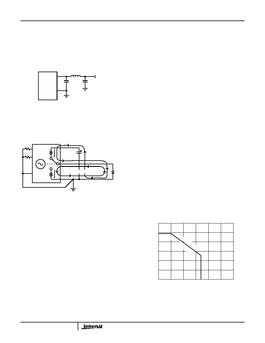
Supply Bypassing and Grounding
The resistance of bypass-capacitors and the inductance of
bonding wires prevent perfect bypass action, and 150mV
P-P
noise on the power lines is common. There needs to be a
lossy bead inductance and secondary bypass on the supply
side to control signals from propagating down the wires.
Figure 20 shows the typical connection.
Also important is circuit-board layout. At the EL6203's
operating frequencies, even the ground plane is not low-
impedance. High frequency current will create voltage drops
in the ground plane. Figure 21 shows the output current
loops.
For the pushing current loop, the current flows through the
bypass capacitor, into the EL6203 supply pin, out the I
OUT
pin to the laser, and from the laser back to the decoupling
capacitor. This loop should be small.
For the pulling current loop, the current flows into the I
OUT
pin, out of the ground pin, to the laser cathode, and from the
laser diode back to the I
OUT
pin. This loop should also be
small.
Power Dissipation
With the high output drive capability, the EL6203 is possible
to exceed the 125∞C "absolute-maximum junction
temperature" under certain conditions. Therefore, it is
important to calculate the maximum junction temperature for
the application to determine if the conditions need to be
modified for the oscillator to remain in the safe operating
area.
The maximum power dissipation allowed in a package is
determined according to:
where
P
DMAX
= Maximum power dissipation in the package
T
JMAX
= Maximum junction temperature
T
AMAX
= Maximum ambient temperature
JA
= Thermal resistance of the package
The supply current of the EL6203 depends on the peak-to-
peak output current and the operating frequency which are
determined by resistors R
AMP
and R
FREQ
. The supply
current can be predicted approximately by the following
equation:
The power dissipation can be calculated from the following
equation:
Here, V
SUP
is the supply voltage. Figures 22 and 23 provide
a convenient way to see if the device will overheat. The
maximum safe power dissipation can be found graphically,
based on the package type and the ambient temperature. By
using the previous equation, it is a simple matter to see if P
D
exceeds the device's power derating curve. To ensure
proper operation, it is important to observe the
recommended derating curve shown in Figures 22 and 23. A
flex circuit may have a higher
JA
, and lower power
dissipation would then be required.
FIGURE 20. RECOMMENDED SUPPLY BYPASSING
+5V
V
S
L Series: 70
reactance at 300MHz
0.1µF
CHIP
EL6203
GND
0.1µF
CHIP
FIGURE 21. OUTPUT CURRENT LOOPS
SINKING CURRENT LOOP
SOURCING CURRENT LOOP
SUPPLY
BYPASS
LASER
DIODE
R
FREQ
R
AMP
GND
P
DMAX
T
JMAX
- T
AMAX
JA
---------------------------------------------
=
I
SUP
31.25mA 1k
◊
R
AMP
-------------------------------------------
30mA 1k
◊
R
FREQ
----------------------------------
0.6mA
+
+
=
P
D
V
SUP
I
SUP
◊
=
FIGURE 22. PACKAGE POWER DISSIPATION vs
AMBIENT TEMPERATURE
0.6
0.5
0.4
0.3
0.2
0.1
0
0
25
50
75
100
125
150
AMBIENT TEMPERATURE (∞C)
P
O
WE
R DISS
IPAT
I
O
N (W
)
85
JEDEC JESD51-3 LOW EFFECTIVE THERMAL
CONDUCTIVITY TEST BOARD
488mW
5-P
in S
OT
-23
JA =2
56∞C
/W
EL6203

10
All Intersil U.S. products are manufactured, assembled and tested utilizing ISO9000 quality systems.
Intersil Corporation's quality certifications can be viewed at www.intersil.com/design/quality
Intersil products are sold by description only. Intersil Corporation reserves the right to make changes in circuit design, software and/or specifications at any time without
notice. Accordingly, the reader is cautioned to verify that data sheets are current before placing orders. Information furnished by Intersil is believed to be accurate and
reliable. However, no responsibility is assumed by Intersil or its subsidiaries for its use; nor for any infringements of patents or other rights of third parties which may result
from its use. No license is granted by implication or otherwise under any patent or patent rights of Intersil or its subsidiaries.
For information regarding Intersil Corporation and its products, see www.intersil.com
FIGURE 23. PACKAGE POWER DISSIPATION vs
AMBIENT TEMPERATURE
0.6
0.5
0.4
0.3
0.2
0.1
0
0
25
50
75
100
125
150
AMBIENT TEMPERATURE (∞C)
POW
E
R
D
I
SSIP
A
TION
(
W
)
85
543mW
5-P
in S
OT
-23
JA =
230
∞C
/W
JEDEC JESD51-7 HIGH EFFECTIVE THERMAL
CONDUCTIVITY TEST BOARD
EL6203