 | ÐлекÑÑоннÑй компоненÑ: EL6207 | СкаÑаÑÑ:  PDF PDF  ZIP ZIP |
Äîêóìåíòàöèÿ è îïèñàíèÿ www.docs.chipfind.ru
1
®
FN7221
CAUTION: These devices are sensitive to electrostatic discharge; follow proper IC Handling Procedures.
1-888-INTERSIL or 321-724-7143
|
Intersil (and design) is a registered trademark of Intersil Americas Inc.
Copyright © Intersil Americas Inc. 2003. All Rights Reserved. Elantec is a registered trademark of Elantec Semiconductor, Inc.
All other trademarks mentioned are the property of their respective owners.
EL6207
Dual Laser Driver Oscillator
The EL6207 is a dual push-pull
oscillator used to reduce laser noise. It
is optimized for 350MHz operation,
allowing reduced concern for harmonic EMI. It uses the
standard interface to existing ROM controllers. The
frequency and amplitude are each set with a separate
resistor connected to ground, for each output. The tiny
package and harmonic reduction allow the part to be placed
close to a laser with low RF emissions.
If the voltage at both I
OUT
pins is less than 1.0V, the chip will
be powered down and not oscillate. If the voltage at either
I
OUT
pin is above 1.4V, the chip will be powered up and
oscillating. If both I
OUT
pins are above 1.4V, the chip will
also be powered down, and not oscillate.
The current drawn by the oscillator consists of a small utility
current, plus the peak oscillator amplitude in the positive
cycle, which is routed to the enabled I
OUT
pin. In the
negative cycle the oscillator subtracts peak oscillator
amplitude from the laser APC current.
The part operates from a single 5V supply, and is specified
for operation from 0
°
C to +85°C.
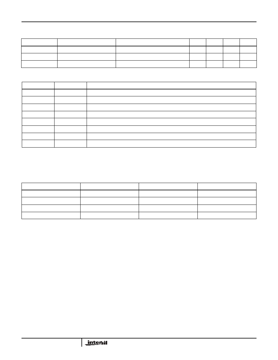
Pinout
EL6207
(8-PIN LPP)
TOP VIEW
Features
· Low power dissipation
· User-selectable frequency from 100MHz to 600MHz
controlled with a single resistor for each laser
· User-specified amplitude from 10mA
PK-PK
to 100mA
PK
controlled with a single resistor for each output
· Auto turn-off threshold
· Soft edges for reduced EMI
· Small 8-pin LPP package
Applications
· Combi drive using dual laser
1
2
3
4
8
7
6
5
VDD
IOUT1
GND
IOUT2
RAMP1
RAMP2
RFREQ1
RFREQ
Ordering Information
PART
NUMBER
PACKAGE
TAPE & REEL
PKG. NO.
EL6207CL
8-Pin LPP
-
MDP0047
Data Sheet
October 10, 2002
2
Absolute Maximum Ratings
(T
A
= 25°C)
Voltages Applied to:
V
DD
. . . . . . . . . . . . . . . . . . . . . . . . . . . . . . . . . -0.5V to +6.0V
I
OUT
. . . . . . . . . . . . . . . . . . . . . . . . . . . . . . . . -0.5V to +6.0V
R
FREQ
, R
AMP
. . . . . . . . . . . . . . . . . . . . . . . . . -0.5V to +6.0V
Operating Ambient Temperature Range . . . . . . . . . . . 0°C to +85°C
Maximum Die Temperature . . . . . . . . . . . . . . . . . . . . . . . . . . +150°C
Storage Temperature Range . . . . . . . . . . . . . . . . . . -65°C to +150°C
I
OUT
Current . . . . . . . . . . . . . . . . . . . . . . . . . . . . . . . . 100mA
PK-PK
Power Dissipation (maximum) . . . . . . . . . . . . . . . . . . . . See Curves
CAUTION: Stresses above those listed in "Absolute Maximum Ratings" may cause permanent damage to the device. This is a stress only rating and operation of the
device at these or any other conditions above those indicated in the operational sections of this specification is not implied.
IMPORTANT NOTE: All parameters having Min/Max specifications are guaranteed. Typical values are for information purposes only. Unless otherwise noted, all tests
are at the specified temperature and are pulsed tests, therefore: T
J
= T
C
= T
A
Supply & Reference Voltage Characteristics
V
DD
= +5V, T
A
= 25°C, R
L
= 10
, R
FREQ
= 5210
(FREQ = 360MHz), R
AMP
=
2540
(Amp = 50mA
P-P
measured at 95MHz), V
OUT
= 2.2V (One channel active)
PARAMETER
DESCRIPTION
CONDITIONS
MIN
TYP
MAX
UNIT
PSOR
Power Supply Operating Range
4.5
5.5
V
I
SO
Supply Current Disabled
V
OUT1
and V
OUT2
< 1.3V
550
750
µA
I
STYP
Supply Current Typical Conditions
R
FREQ
= 5.21k
,
R
AMP
= 2.54k
, V
OUT1
or
V
OUT2
>1.4V
17
22
mA
I
SLO
Supply Current Low Conditions
R
FREQ
= 18.2k
, R
AMP
= 13k
, V
OUT1
or
V
OUT2
>1.4V
6
mA
I
SHI
Supply Current High Conditions
R
FREQ
= 3.05k
,
R
AMP
= 1.3k
, V
OUT1
or
V
OUT2
>1.4
32
mA
V
CUTOFF
Output Cutoff Voltage
Average voltage at cutoff
1.1
1.4
V
V
FREQ
Voltage at R
FREQ
Pin
1.27
V
V
RAMP
Voltage on R
AMP
Pin
1.27
V
Oscillator Characteristics
V
DD
= +5V, T
A
= 25°C, R
L
= 10
, R
FREQ
= 5210
(FREQ = 360MHz), R
AMP
= 2540
(Amp = 50mA
P-P
measured at 100MHz), V
OUT
= 2.2V (One channel active)
PARAMETER
DESCRIPTION
CONDITIONS
MIN
TYP
MAX
UNIT
F
OSC
Frequency Tolerance
Unit-unit frequency variation
310
360
410
MHz
F
HIGH
Frequency Range High
R
FREQ
= 3.0k
600
MHz
F
LOW
Frequency Range Low
R
FREQ
= 18.2k
100
MHz
TC
OSC
Frequency Temperature Sensitivity
-40°C to +85°C ambient
50
ppm/°C
PSRR
OSC
Frequency Change
F/F
V
DD
from 4.5V to 5.5V
1
%
Driver Characteristics
V
DD
= +5V, T
A
= 25°C, R
L
= 10
, R
FREQ
= 18.2k
(FREQ = 100MHz), R
AMP
= 2540
(Amp = 50mA
P-P
measured at 100MHz), V
OUT
= 2.2V (One channel active)
PARAMETER
DESCRIPTION
CONDITIONS
MIN
TYP
MAX
UNIT
AMP
HIGH
Amplitude Range High
R
AMP
= 1.27k
100
mA
P-P
AMP
LOW
Amplitude Range Low
R
AMP
= 12.7k
10
mA
P-P
IOFF
NOM
Average Output Current @ 2.2V
R
FREQ
= 5210
,
10
load, V
OUT
= 2.2V
-4
mA
IOFF
HIGH
Average Output Current @ 2.8V
R
FREQ
= 5210
,
10
load, V
OUT
= 3.0V
-4.8
mA
IOFF
LOW
Average Output Current @ 1.8V
R
FREQ
= 5210
,
10
load, V
OUT
= 1.8V
-3.5
mA
I
OUTP-P
Output Current Tolerance
Defined as on standard deviation
2
%
Duty Cycle
Output Push Time/Cycle Time
R
FREQ
= 5210
43
%
PSRR
AMP
Amplitude Change of Output
I/I
V
DD
from 4.5V to 5.5V
-54
dB
EL6207
3
Recommended Operating Conditions
V
DD
. . . . . . . . . . . . . . . . . . . . . . . . . . . . . . . . . . . . . . . . . . 5V ±10%
V
OUT
. . . . . . . . . . . . . . . . . . . . . . . . . . . . . . . . . . . . . . . . . . . 2V - 3V
R
FREQ
. . . . . . . . . . . . . . . . . . . . . . . . . . . . . . . . . . . . . . . . 3k
(min)
R
AMP
. . . . . . . . . . . . . . . . . . . . . . . . . . . . . . . . . . . . . . . 1.3k
(min)
F
OSC
. . . . . . . . . . . . . . . . . . . . . . . . . . . . . . . . . . . . . . . .80-600MHz
A
OSC
. . . . . . . . . . . . . . . . . . . . . . . . . . . . . . . . . . . . 10-100mA
PK-PK
T
ON
Auto Turn-on Time
Output voltage step from 0V to 2.2V
15
µs
T
OFF
Auto Turn-off Time
Output voltage step from 2.2V to 0V
0.5
µs
IN
OUT
I
OUT
Current Output Noise Density R
FREQ
= 5210
,
F
MEASURE
= 10MHz
2.5
nA/
Hz
Driver Characteristics
V
DD
= +5V, T
A
= 25°C, R
L
= 10
, R
FREQ
= 18.2k
(FREQ = 100MHz), R
AMP
= 2540
(Amp = 50mA
P-P
measured at 100MHz), V
OUT
= 2.2V (One channel active) (Continued)
PARAMETER
DESCRIPTION
CONDITIONS
MIN
TYP
MAX
UNIT
Pin Descriptions
PIN NAME
PIN TYPE
PIN DESCRIPTION
1
V
DD
Positive power for laser driver (4.5V - 5.5V)
2
IOUT1
Current output to laser anode
3
GND
Chip ground pin (0V)
4
IOUT1
Current output to laser anode
5
RFREQ2
Set pin for oscillator frequency
6
RFREQ1
Set pin for oscillator frequency
7
RAMP2
Amplitude control input pin
8
RAMP1
Amplitude control input pin
I
OUT
Control
V
OUT1
V
OUT2
I
OUT
I
OUT
Less than V
CUTOFF
Less than V
CUTOFF
OFF
OFF
Less than V
CUTOFF
More than V
CUTOFF
OFF
Normal Operation
More than V
CUTOFF
Less than V
CUTOFF
Normal Operation
OFF
More than V
CUTOFF
More than V
CUTOFF
OFF
OFF
EL6207
4
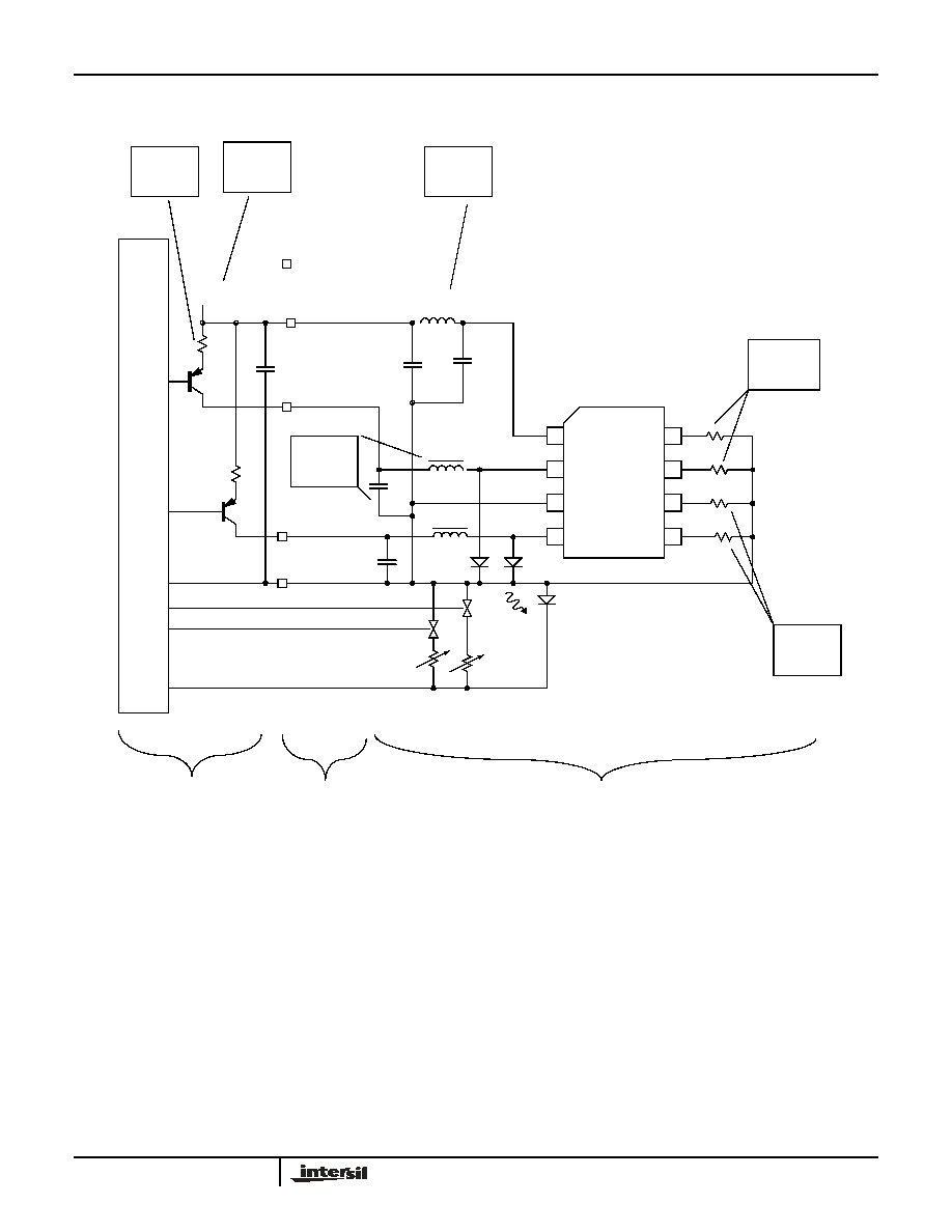
Block Diagram
Controller
Frequency
Setting
Resistor
EMI
Reduction
Supply Filter
Gain
Setting
Resistor
Typical
ROM Laser
Driver
Laser
Rear
Photodiode
BEAD
+5V
GND
4.7µF
Amplitude
Setting
Resistors
0.1uF
0.1uF
PNP
BEAD
0.1uF
EMI
Reduction
Filters
Main Board
On Pickup
Flex
1
2
3
7
6
VDD
RAMP1
IOUT1
RAMP2
GND
RFREQ1
8
4
IOUT2
5
RFREQ2
BEAD
Calibration
Pots
PNP
0.1uF
EL6207
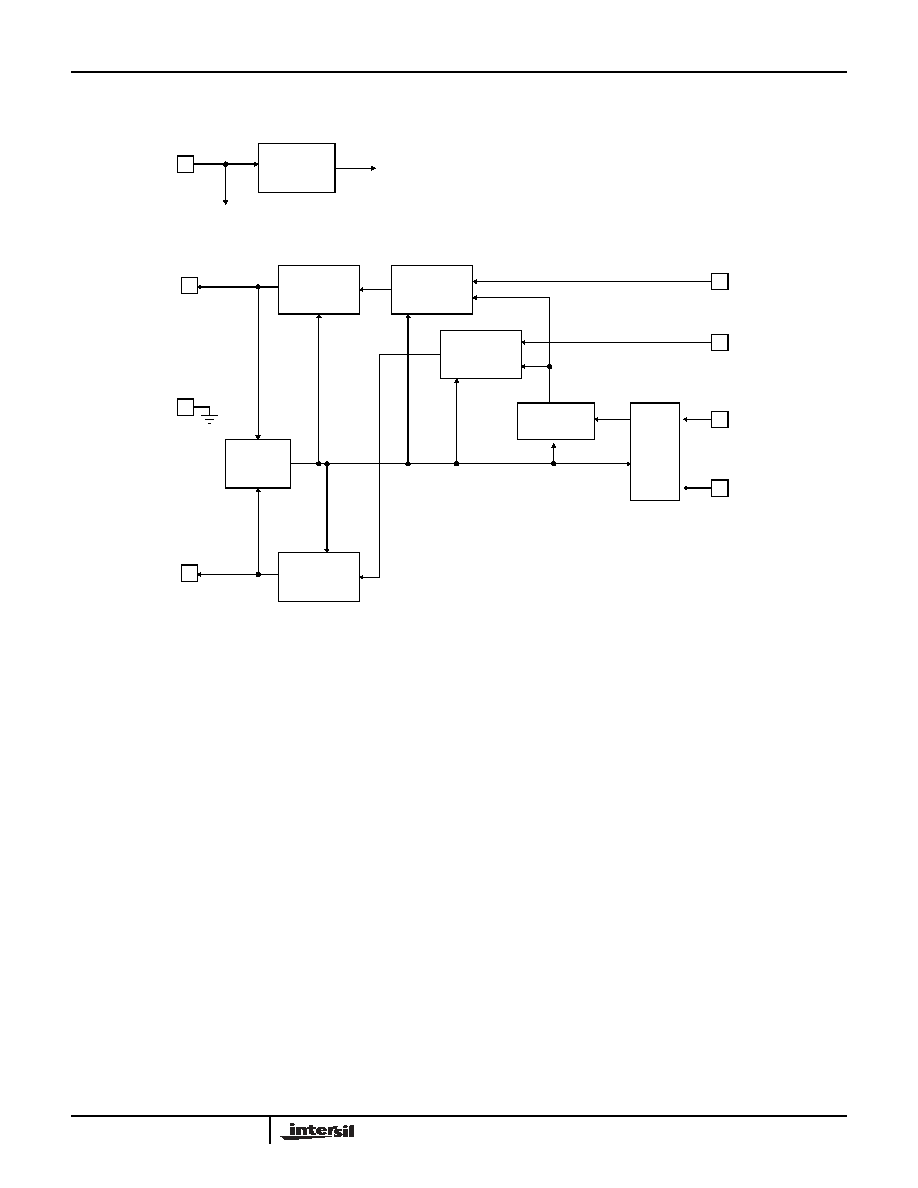
5
Block Diagram
(Continued)
OSCILLATOR
AMPLIFIER
DRIVER
1
2
3
8
6
RFREQ 1
RAMP 1
VDD
GND
IOUT 1
BAND GAP
REFERENCE
AMPLIFIER
DRIVER
4
7
RAMP 2
IOUT 2
5
RFREQ 2
ENABLE
LOGIC
SELECT
EL6207