 | –≠–ª–µ–∫—Ç—Ä–æ–Ω–Ω—ã–π –∫–æ–º–ø–æ–Ω–µ–Ω—Ç: EL6208 | –°–∫–∞—á–∞—Ç—å:  PDF PDF  ZIP ZIP |

1
Æ
FN7374
CAUTION: These devices are sensitive to electrostatic discharge; follow proper IC Handling Procedures.
1-888-INTERSIL or 321-724-7143
|
Intersil (and design) is a registered trademark of Intersil Americas Inc.
Copyright © Intersil Americas Inc. 2003. All Rights Reserved. Elantec is a registered trademark of Elantec Semiconductor, Inc.
All other trademarks mentioned are the property of their respective owners.
EL6208
Dual Push-Pull Laser Driver Oscillator
The EL6208 is a dual push-pull
oscillator used to reduce laser noise in
twin laser diodes. It uses the standard
interface to existing ROM controllers. The frequency and
amplitude are both set with a separate resistor connected to
ground. The tiny package and harmonic reduction allow the
part to be placed close to a laser with low RF emissions. An
auto turn-off feature allows activates the oscillator only when
the APC current is applied.
If the APC current is reduced such that the average laser
voltage drops to less than 1.1V, the output and oscillator are
disabled, reducing power consumption to a minimum.
The current drawn by the oscillator consists of a small utility
current, plus the peak output amplitude in the positive cycle.
In the negative cycle the oscillator subtracts peak output
amplitude from the laser APC current. The waveform is
filtered to reduce EMI emissions.
The EL6208 operates from a signal +5V supply. Power
consumption is very low. The EL6208 part is available in the
space-saving 6-pin SOT-23 package and is specified for
operation from 0∞C to +70∞C.
Features
∑ Low power dissipation
∑ User-selectable frequency from 60MHz to 600MHz
controlled with a single resistor
∑ User-specified amplitude from 10mA
PK-PK
to
100mA
PK-PK
controlled with a single resistor
∑ Auto turn-off threshold
∑ Soft edges for reduced EMI
∑ Small 6-pin SOT-23 package
Applications
∑ CD-DVD ROM drives
Pinout
EL6208
(6-PIN SOT-23)
TOP VIEW
Ordering Information
PART NUMBER
PACKAGE
TAPE &
REEL
PKG. DWG. #
EL6208CW-T7
6-Pin SOT-23
7" (3K pcs)
MDP0038
EL6208CW-T7A
6-Pin SOT-23
7" (250 pcs)
MDP0038
1
2
3
6
4
5
VDD
RFREQ
RAMP
IOUT2
GND
IOUT1
Data Sheet
July 23, 2003

2
Absolute Maximum Ratings
(T
A
= 25∞C)
Recommended Operating Conditions
Voltages Applied to:
V
DD
. . . . . . . . . . . . . . . . . . . . . . . . . . . . . . . . . . . -0.5V to +6.0V
I
OUT
. . . . . . . . . . . . . . . . . . . . . . . . . . . . . . . . . . . -0.5V to +6.0V
R
FREQ
, R
AMP
. . . . . . . . . . . . . . . . . . . . . . . . . . . -0.5V to +6.0V
Operating Ambient Temperature Range . . . . . . . . . . . 0∞C to +70∞C
Maximum Junction Temperature . . . . . . . . . . . . . . . . . . . . . . +150∞C
Storage Temperature Range . . . . . . . . . . . . . . . . . .-65∞C to +150∞C
Output Current . . . . . . . . . . . . . . . . . . . . . . . . . . . . . . . 100mA
PK-PK
Power Dissipation (max) . . . . . . . . . . . . . . . . . . . . . . . . See Curves
V
DD
. . . . . . . . . . . . . . . . . . . . . . . . . . . . . . . . . . . . . . . . . . .5V ±10%
V
OUT
. . . . . . . . . . . . . . . . . . . . . . . . . . . . . . . . . . . . . . . . . . . 2V - 3V
R
FREQ
. . . . . . . . . . . . . . . . . . . . . . . . . . . . . . . . . . . . . . . . 3K
(min)
R
AMP
. . . . . . . . . . . . . . . . . . . . . . . . . . . . . . . . . . . . . . 1.25k
(min)
F
OSC
. . . . . . . . . . . . . . . . . . . . . . . . . . . . . . . . . . . . . . . .60-600MHz
I
OUT
. . . . . . . . . . . . . . . . . . . . . . . . . . . . . . . . . . . . . 10-100mA
PK-PK
CAUTION: Stresses above those listed in "Absolute Maximum Ratings" may cause permanent damage to the device. This is a stress only rating and operation of the
device at these or any other conditions above those indicated in the operational sections of this specification is not implied.
IMPORTANT NOTE: All parameters having Min/Max specifications are guaranteed. Typical values are for information purposes only. Unless otherwise noted, all tests
are at the specified temperature and are pulsed tests, therefore: T
J
= T
C
= T
A
Supply & Reference Voltage Characteristics
V
DD
= +5V, T
A
= 25∞C, R
L
= 10
, R
FREQ
= 5210
(F
OSC
= 360MHz), R
AMP
=
2540
(I
OUT
= 50mA
P-P
measured at 60MHz), V
OUT
= 2.2V
PARAMETER
DESCRIPTION
CONDITIONS
MIN
TYP
MAX
UNIT
PSOR
Power Supply Operating Range
4.5
5.5
V
I
SO
Supply Current Disabled
V
OUT
< V
CUTOFF
280
440
µA
I
STYP
Supply Current Typical Conditions
R
FREQ
= 5.21k
,
R
AMP
= 2.54k
20
23
mA
I
SLO
Supply Current Low Conditions
R
FREQ
= 18.2k
, R
AMP
= 12.7k
5.4
mA
I
SHI
Supply Current High Conditions
R
FREQ
= 3.3k
,
R
AMP
= 1.27k
36.8
mA
V
FREQ
Voltage at R
FREQ
Pin
1.27
V
V
RAMP
Voltage on R
AMP
Pin
1.27
V
V
CUTOFF
Monitoring Voltage of I
OUT
Pin
1.1
1.4
V
Oscillator Characteristics
V
DD
= +5V, T
A
= 25∞C, R
L
= 10
, R
FREQ
= 5210
(F
OSC
= 360MHz), R
AMP
= 2540
(I
OUT
= 50mA
P-P
measured at 60MHz), V
OUT
= 2.2V
PARAMETER
DESCRIPTION
CONDITIONS
MIN
TYP
MAX
UNIT
F
OSC
Frequency Tolerance
Unit-unit frequency variation
310
358
400
MHz
F
HIGH
Frequency Range High
R
FREQ
= 3.3k
566
MHz
F
LOW
Frequency Range Low
R
FREQ
= 18.2k
100
MHz
TC
OSC
Frequency Temperature Sensitivity
0∞C to +70∞C ambient
50
ppm/∞C
PSRR
OSC
Frequency Change
F/F
V
DD
from 4.5V to 5.5V
1
%
Driver Characteristics
V
DD
= +5V, T
A
= 25∞C, R
L
= 10
, R
FREQ
= 30.5k
(F
OSC
= 60MHz), R
AMP
= 2540
(I
OUT
= 50mA
P-P
measured at 60MHz), V
OUT
= 2.2V
PARAMETER
DESCRIPTION
CONDITIONS
MIN
TYP
MAX
UNIT
AMP
HIGH
Amplitude Range High
R
AMP
= 1.27k
100
mA
P-P
AMP
LOW
Amplitude Range Low
R
AMP
= 12.7k
10
mA
P-P
IOS
NOM
Offset Current @ 2.2V
R
FREQ
= 5210
,
V
OUT
= 2.2V
-4
mA
IOS
HIGH
Offset Current @ 2.8V
R
FREQ
= 5210
,
V
OUT
= 2.8V
-4.8
mA
IOS
LOW
Offset Current @ 1.8V
R
FREQ
= 5210
,
V
OUT
= 1.8V
-3.5
mA
I
OUTP-P
Output Current Tolerance
Defined as one standard deviation
2
%
Duty Cycle
Output Push Time/Cycle Time
R
FREQ
= 5210
43
%
PSRR
AMP
Amplitude Change of Output
I/I
V
DD
from 4.5V to 5.5V
-54
dB
EL6208

3
T
ON
Auto Turn-on Time
Output voltage step from 0V to 2.2V
15
µs
T
OFF
Auto Turn-off Time
Output voltage step from 2.2V to 0V
0.5
µs
IOUT
N
Output Current Noise Density
R
FREQ
= 5210
,
measured @ 10MHz
2.5
nA/
Hz
Driver Characteristics
V
DD
= +5V, T
A
= 25∞C, R
L
= 10
, R
FREQ
= 30.5k
(F
OSC
= 60MHz), R
AMP
= 2540
(I
OUT
= 50mA
P-P
measured at 60MHz), V
OUT
= 2.2V (Continued)
PARAMETER
DESCRIPTION
CONDITIONS
MIN
TYP
MAX
UNIT
Pin Descriptions
PIN NAME
PIN TYPE
PIN DESCRIPTION
1
VDD
Positive power for laser driver (4.5V - 5.5V)
2
RFREQ
Set pin for oscillator frequency
3
RAMP
Set pin for output current amplitude
4
IOUT1
Current output to laser diode
5
GND1
Chip ground pin (0V for output)
6
IOUT2
Current output to laser diode
I
OUT
Control
V
OUT
I
OUT
Less than V
CUTOFF
OFF
More than V
CUTOFF
Normal Operation
EL6208
4
Typical Performance Curves
V
DD
= 5V, T
A
= 25∞C, R
L
= 10
, R
FREQ
= 5.21k
, R
AMP
= 2.54k
, V
OUT
= 2.2V unless otherwise specified.
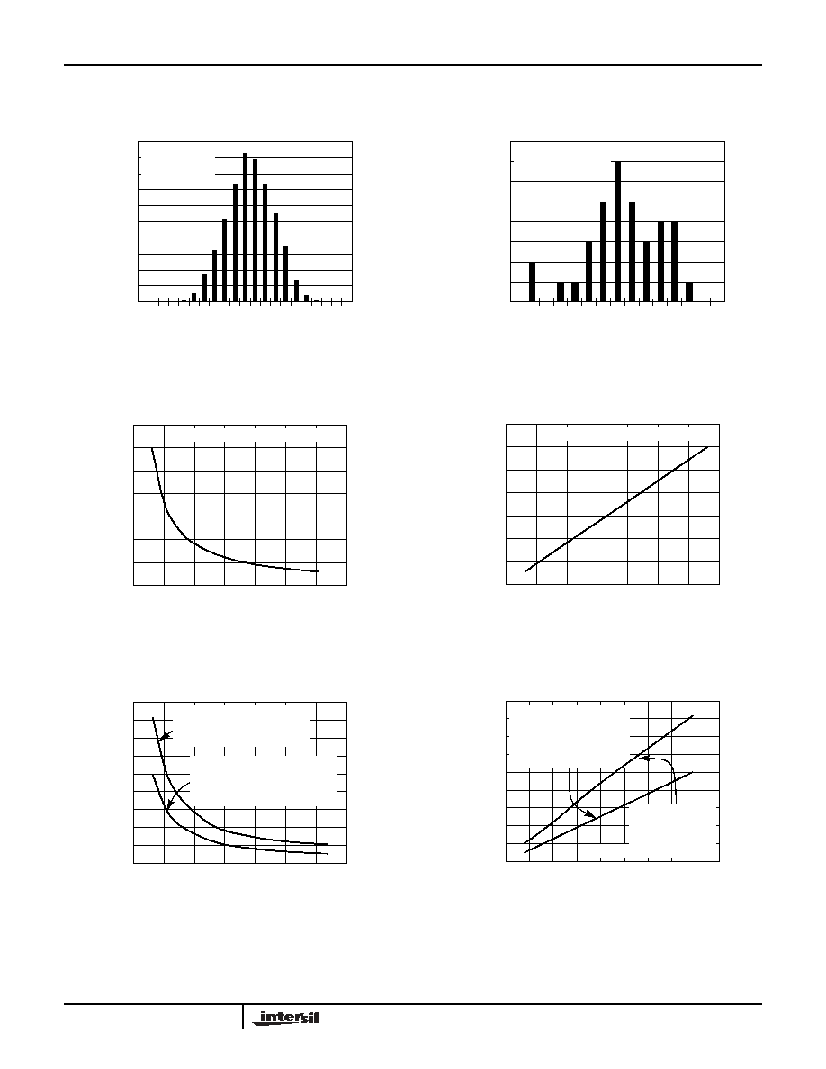
FIGURE 1. FREQUENCY DISTRIBUTION
FIGURE 2. FREQUENY DRIFT with TEMPERATURE
FIGURE 3. FREQUENCY vs R
FREQ
FIGURE 4. FREQUENCY vs 1 / R
FREQ
FIGURE 5. OUTPUT CURRENT vs R
AMP
FIGURE 6. OUTPUT CURRENT vs 1 / R
AMP
NUM
BER OF
P
ART
S
0
100
500
FREQUENCY (MHz)
32
0
32
8
34
4
36
0
37
6
33
6
35
2
36
8
200
300
400
38
4
39
2
40
0
TYPICAL
PRODUCTION
DISTORTION
NUM
BER OF
P
ART
S
0
1
8
FREQUENCY TC (ppm/∞C)
6
30
54
18
42
3
5
7
66
78
90
MEASURED FROM
-40∞C TO +85∞C
2
4
6
F
R
EQUENCY (
M
Hz)
0
200
400
500
600
700
R
FREQ
(k
)
0
5
15
25
35
10
20
30
100
300
FREQ = 1824 * 1k
/ R
FREQ
(MHz)
F
R
EQUENCY (
M
Hz)
0
200
400
500
600
700
1k
/ R
FREQ
0
0.05
0.15
0.25
0.35
0.1
0.2
0.3
100
300
FREQ = 1824 * 1k
/ R
FREQ
(MHz)
OUT
P
UT
CURRENT
(
m
A)
0
40
80
120
160
180
R
AMP
(k
)
0
2
6
10
14
4
8
12
20
60
100
140
AMPLITUDE PK-PK = 127 * 1k
/
R
AMP
(mA) MEASURED
@60MHz (OVER-SHOOT NOT
INCLUDED)
I
OUT PK-PK
MEASURED
@60/350/600MHz
(OVER-SHOOT INCLUDED)
O
U
T
P
UT
CURRENT
(
m
A)
0
40
80
120
160
180
1k
/ R
AMP
0
0.1
0.5
0.7
0.9
0.3
0.6
0.8
20
60
100
140
0.2
0.4
I
OUT PK-PK
MEASURED
@60/350/600MHz
AMPLITUDE PK-PK = 127 *
1k
/ R
AMP
(mA)
MEASURED
@60MHz (OVER-SHOOT
NOT INCLUDED)
(OVER-SHOOT INCLUDED)
EL6208

5
FIGURE 7. SUPPLY CURRENT vs R
FREQ
FIGURE 8. SUPPLY CURRENT vs R
AMP
FIGURE 9. FREQUENCY vs SUPPLY VOLTAGE
FIGURE 10. PEAK-TO-PEAK OUTPUT CURRENT vs SUPPLY
VOLTAGE
FIGURE 11. SUPPLY CURRENT vs SUPPLY VOLTAGE
FIGURE 12. FREQUENCY vs TEMPERATURE
Typical Performance Curves
(Continued)
V
DD
= 5V, T
A
= 25∞C, R
L
= 10
, R
FREQ
= 5.21k
, R
AMP
= 2.54k
, V
OUT
= 2.2V unless otherwise specified.
SUPP
L
Y
CURRENT
(
m
A)
0
40
50
R
FREQ
(k
)
0
5
15
25
30
10
20
30
R
AMP
=1k
R
AMP
=2.54k
R
AMP
=20k
R
AMP
=5k
R
AMP
=10k
20
10
SUPP
L
Y
CURRENT
(
m
A)
0
35
45
R
AMP
(k
)
0
5
15
25
30
10
20
10
30
40
5
R
FREQ
=2.9k
R
FREQ
=5.21k
R
FREQ
=10k
R
FREQ
=30k
R
FREQ
=20k
15
25
20
F
R
EQUENCY (
M
Hz
)
340
345
355
360
SUPPLY VOLTAGE (V)
4.4
4.6
4.8
5.2
5.6
5
5.4
350
I
OU
T
PK-
P
K
(m
A
)
80
85
95
100
SUPPLY VOLTAGE (V)
4.4
4.6
4.8
5.2
5.6
5
5.4
90
SUPPL
Y CURRENT
(
m
A)
17
18
20
21
SUPPLY VOLTAGE (V)
4.4
4.6
4.8
5.2
5.6
5
5.4
19
F
R
EQ
UENCY
(
M
Hz)
300
320
380
400
AMBIENT TEMPERATURE (∞C)
-50
0
150
50
100
340
360
EL6208