1
Æ
FN7113.1
EL7104
High Speed, Single Channel, Power
MOSFET Driver
The EL7104 is a matched driver IC that improves the
operation of the industry-standard TC-4420/29 clock drivers.
The Elantec version is a very high speed driver capable of
delivering peak currents of 1A into highly capacitive loads.
The high speed performance is achieved by means of a
proprietary "Turbo-Driver" circuit that speeds up input stages
by tapping the wider voltage swing at the output. Improved
speed and drive capability are enhanced by matched rise
and fall delay times. These matched delays maintain the
integrity of input-to-output pulse-widths to reduce timing
errors and clock skew problems. This improved performance
is accompanied by a 10-fold reduction in supply currents
over bipolar drivers, yet without the delay time problems
commonly associated with CMOS drivers.
The EL7104 is available in 8-pin SO and 8-pin PDIP
packages and is specified for operation over the full -40∞C to
+85∞C temperature range.
Features
∑ Industry-standard driver replacement
∑ Improved response times
∑ Matched rise and fall times
∑ Reduced clock skew
∑ Low output impedance
∑ Low input capacitance
∑ High noise immunity
∑ Improved clocking rate
∑ Low supply current
∑ Wide operating range
∑ Separate drain connections
∑ Pb-Free available (RoHS compliant)
Applications
∑ Clock/line drivers
∑ CCD drivers
∑ Ultrasound transducer drivers
∑ Power MOSFET drivers
∑ Switch mode power supplies
∑ Resonant charging
∑ Cascoded drivers
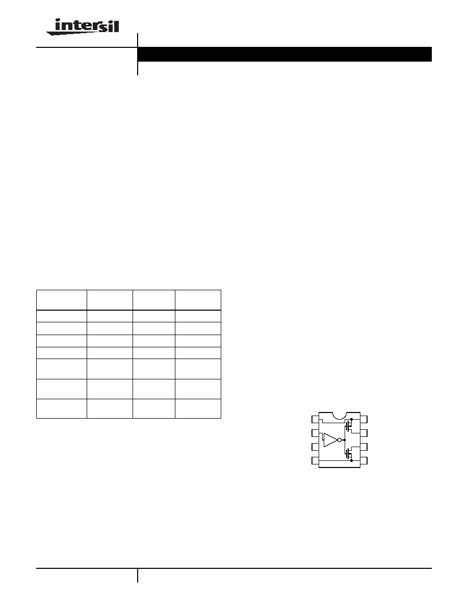
Pinout
EL7104
(8-PIN SO, PDIP)
TOP VIEW
Ordering Information
PART
NUMBER
PACKAGE
TAPE &
REEL
PKG. DWG. #
EL7104CN
8-Pin PDIP
-
MDP0031
EL7104CS
8-Pin SO
-
MDP0027
EL7104CS-T7
8-Pin SO
7"
MDP0027
EL7104CS-T13
8-Pin SO
13"
MDP0027
EL7104CSZ
(See Note)
8-Pin SO
(Pb-free)
-
MDP0027
EL7104CSZ-T7
(See Note)
8-Pin SO
(Pb-free)
7"
MDP0027
EL7104CSZ-T13
(See Note)
8-Pin SO
(Pb-free)
13"
MDP0027
NOTE: Intersil Pb-free products employ special Pb-free material sets;
molding compounds/die attach materials and 100% matte tin plate
termination finish, which are RoHS compliant and compatible with
both SnPb and Pb-free soldering operations. Intersil Pb-free products
are MSL classified at Pb-free peak reflow temperatures that meet or
exceed the Pb-free requirements of IPC/JEDEC J STD-020.
1
2
3
4
8
7
6
5
V+
IN
NC
GND
V+
P_OUT
N_OUT
GND
Data Sheet
May 6, 2005
CAUTION: These devices are sensitive to electrostatic discharge; follow proper IC Handling Procedures.
1-888-INTERSIL or 1-888-352-6832
|
Intersil (and design) is a registered trademark of Intersil Americas Inc.
Copyright Intersil Americas Inc. 2003, 2005. All Rights Reserved
All other trademarks mentioned are the property of their respective owners.

2
IMPORTANT NOTE: All parameters having Min/Max specifications are guaranteed. Typ values are for information purposes only. Unless otherwise noted, all tests are
at the specified temperature and are pulsed tests, therefore: T
J
= T
C
= T
A
Absolute Maximum Ratings
(T
A
= 25∞C)
Supply (V+ to GND) . . . . . . . . . . . . . . . . . . . . . . . . . . . . . . . . . 16.5V
Input Pins . . . . . . . . . . . . . . . . . . . . . . . . . . -0.3V to +0.3V above V+
Peak Output Current . . . . . . . . . . . . . . . . . . . . . . . . . . . . . . . . . . .4A
Ambient Operating Temperature . . . . . . . . . . . . . . . .-40∞C to +85∞C
Storage Temperature Range . . . . . . . . . . . . . . . . . .-65∞C to +150∞C
Operating Junction Temperature . . . . . . . . . . . . . . . . . . . . . . +125∞C
Power Dissipation
SO . . . . . . . . . . . . . . . . . . . . . . . . . . . . . . . . . . . . . . . . . . .570mW
PDIP. . . . . . . . . . . . . . . . . . . . . . . . . . . . . . . . . . . . . . . . .1050mW
CAUTION: Stresses above those listed in "Absolute Maximum Ratings" may cause permanent damage to the device. This is a stress only rating and operation of the
device at these or any other conditions above those indicated in the operational sections of this specification is not implied.
DC Electrical Specifications
V+
= 15V, T
A
= 25∞C unless otherwise specified.
PARAMETER
DESCRIPTION
CONDITIONS
MIN
TYP
MAX
UNIT
INPUT
V
IH
Logic "1" Input Voltage
2.4
V
I
IH
Logic "1" Input Current
@V+
0.1
10
µA
V
IL
Logic "0" Input Voltage
0.8
V
I
IL
Logic "0" Input Current
@0V
0.1
10
µA
V
HVS
Input Hysteresis
0.3
V
OUTPUT
R
OH
Pull-Up Resistance
I
OUT
= -100mA
1.5
4
R
OL
Pull-Down Resistance
I
OUT
= +100mA
2
4
I
OUT
Output Leakage Current
V+/GND
0.2
10
µA
I
PK
Peak Output Current
Source/Sink
4.0
A
I
DC
Continuous Output Current
Source/Sink
200
mA
POWER SUPPLY
I
S
Power Supply Current
Input = V+
4.5
7.5
mA
V
S
Operating Voltage
4.5
16
V
AC Electrical Specifications
V
= 15V, T
A
= 25∞C unless otherwise specified.
PARAMETER
DESCRIPTION
CONDITIONS
MIN
TYP
MAX
UNIT
SWITCHING CHARACTERISTICS (V
DD
= V
H
= 12V; V
L
= -3V)
t
R
Rise Time
C
L
= 1000pF
7.5
ns
C
L
= 2000pF
10
20
ns
t
F
Fall Time
C
L
= 1000pF
10
ns
C
L
= 2000pF
15
20
ns
t
D-ON
Turn-On Delay Time
See Timing Table
18
25
ns
t
D-OFF
Turn-Off Delay Time
See Timing Table
18
25
ns
EL7104
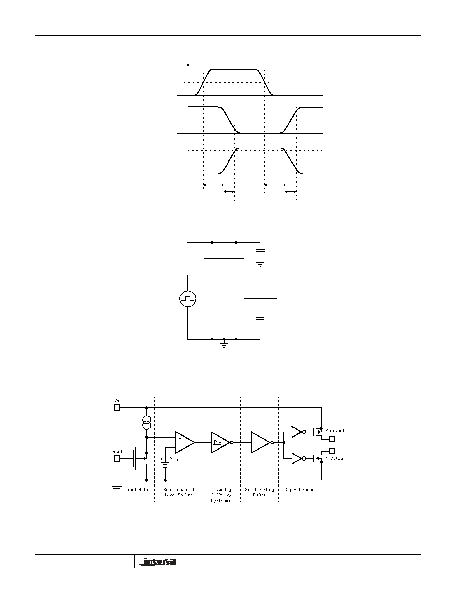
3
Timing Table
Standard Test Configuration
Simplified Schematic
5V
2.5V
90%
10%
90%
10%
0
t
D1
t
D2
t
F
t
R
t
R
t
F
Inverted
Output
EL7114
Non-inverted
Output
EL7104
Input
1
8
2
4
5
6
7
D.U.T.
Input
Signal
Output
Signal
4.7µF
2000pF
EL7104
4
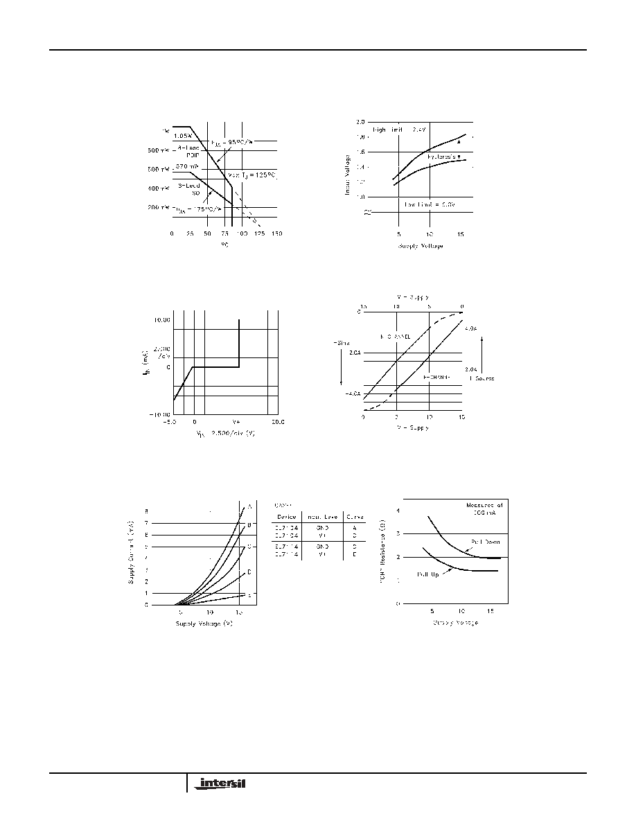
Typical Performance Curves
Max Power/Derating Curves
Switch Threshold vs
Supply Voltage
Peak Drive vs Supply Voltage
Input Current vs Voltage
Quiescent Supply Current
"ON" Resistance vs Supply Voltage
EL7104
5
All Intersil U.S. products are manufactured, assembled and tested utilizing ISO9000 quality systems.
Intersil Corporation's quality certifications can be viewed at www.intersil.com/design/quality
Intersil products are sold by description only. Intersil Corporation reserves the right to make changes in circuit design, software and/or specifications at any time without
notice. Accordingly, the reader is cautioned to verify that data sheets are current before placing orders. Information furnished by Intersil is believed to be accurate and
reliable. However, no responsibility is assumed by Intersil or its subsidiaries for its use; nor for any infringements of patents or other rights of third parties which may result
from its use. No license is granted by implication or otherwise under any patent or patent rights of Intersil or its subsidiaries.
For information regarding Intersil Corporation and its products, see www.intersil.com
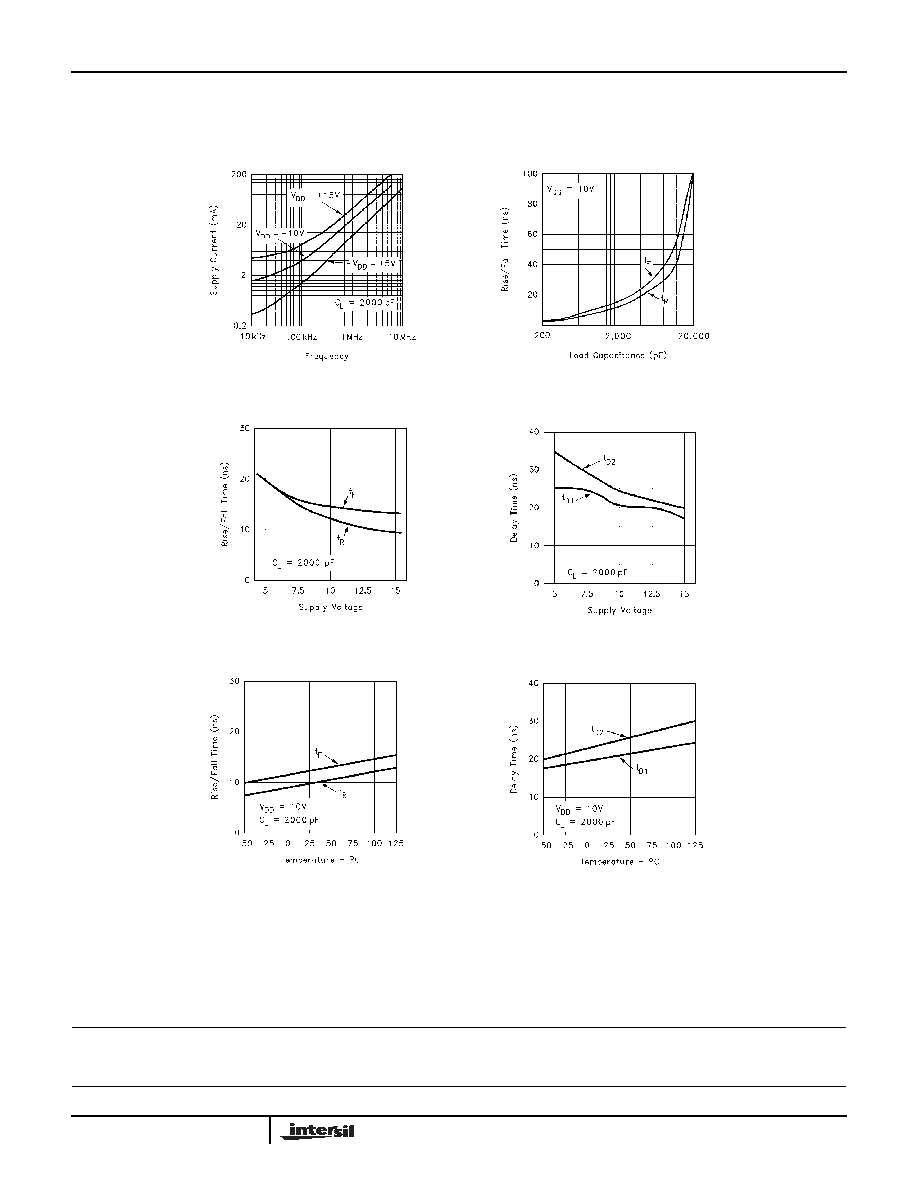
Typical Performance Curves
(Continued)
Average Supply Current vs
Voltage and Frequency
Rise/Fall Time vs Load
Rise/Fall Time vs Supply Voltage
Propagation Delay vs Supply
Voltage
Rise/Fall Time vs Temperature
Rise/Fall Time vs Temperature
EL7104