 | ÐлекÑÑоннÑй компоненÑ: EL7155CN | СкаÑаÑÑ:  PDF PDF  ZIP ZIP |
Äîêóìåíòàöèÿ è îïèñàíèÿ www.docs.chipfind.ru
1
®
FN7279
CAUTION: These devices are sensitive to electrostatic discharge; follow proper IC Handling Procedures.
1-888-INTERSIL or 321-724-7143
|
Intersil (and design) is a registered trademark of Intersil Americas Inc.
Copyright © Intersil Americas Inc. 2003. All Rights Reserved. Elantec is a registered trademark of Elantec Semiconductor, Inc.
All other trademarks mentioned are the property of their respective owners.
EL7155
High Performance Pin Driver
The EL7155 high performance pin
driver with 3-state is suited to many
ATE and level-shifting applications.
The 3.5A peak drive capability makes this part an excellent
choice when driving high capacitance loads.
Output pins OUT
H
and OUT
L
are connected to input pins V
H
and V
L
respectively, depending on the status of the IN pin.
One of the output pins is always in tri-state, except when the
OE pin is active low, in which case both outputs are in 3-
state mode. The isolation of the output FETs from the power
supplies enables V
H
and V
L
to be set independently,
enabling level-shifting to be implemented.
This pin driver has improved performance over existing pin
drivers. It is specifically designed to operate at voltages
down to 0V across the switch elements while maintaining
good speed and on-resistance characteristics.
Available in 8-Pin SO and 8-Pin PDIP packages, the EL7155
is specified for operation over the full -40°C to +85°C
temperature range.
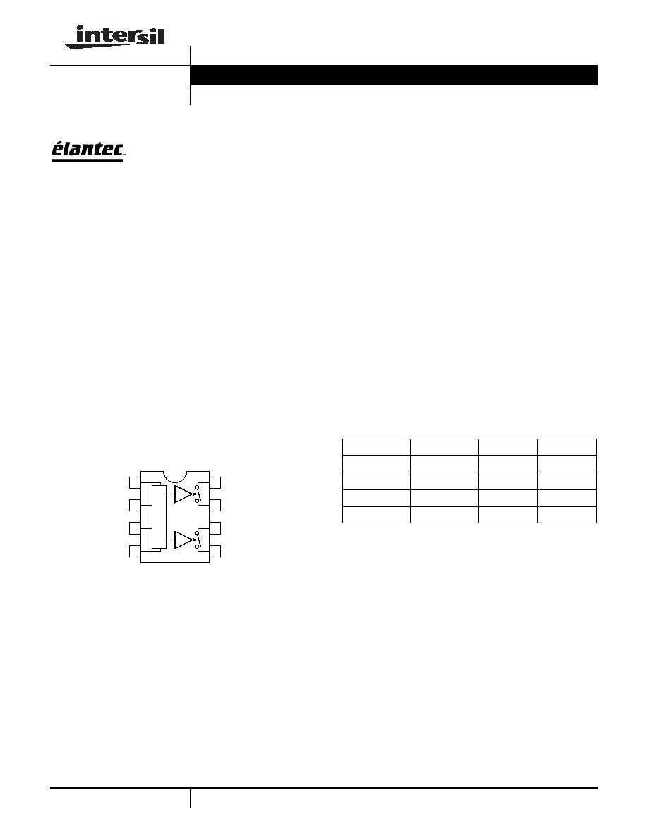
Pinout
EL7155
(8-PIN PDIP, SO)
TOP VIEW
Features
· Clocking speeds up to 40MHz
· 15ns tr/tf at 2000pF C
LOAD
· 0.5ns rise and fall times mismatch
· 0.5ns T
ON
-T
OFF
prop delay mismatch
· 3.5pF typical input capacitance
· 3.5A peak drive
· Low on resistance of 3.5
· High capacitive drive capability
· Operates from 4.5V up to 18V
Applications
· ATE/burn-in testers
· Level shifting
· IGBT drivers
· CCD drivers
1
2
3
4
8
7
6
5
L
o
g
i
c
VS+
OE
IN
GND
VH
OUTH
OUTL
VL
Ordering Information
PART NUMBER
PACKAGE
TAPE & REEL
PKG. NO.
EL7155CN
8-Pin PDIP
-
MDP0031
EL7155CS
8-Pin SO
-
MDP0027
EL7155CS-T7
8-Pin SO
7"
MDP0027
EL7155CS-T13
8-Pin SO
13"
MDP0027
Data Sheet
January 30, 2002
2
Absolute Maximum Ratings
(T
A
= 25°C)
Supply Voltage (V
S
+ to V
L
) . . . . . . . . . . . . . . . . . . . . . . . . . . . .+18V
Input Voltage . . . . . . . . . . . . . . . . . . . . . . . . . . . V
L
-0.3V, V
L
+ +0.3V
Continuous Output Current . . . . . . . . . . . . . . . . . . . . . . . . . . 200mA
Storage Temperature Range . . . . . . . . . . . . . . . . . .-65°C to +150°C
Ambient Operating Temperature . . . . . . . . . . . . . . . . -40°C to +85°C
Operating Junction Temperature . . . . . . . . . . . . . . . . . . . . . . . 125°C
Power Dissipation . . . . . . . . . . . . . . . . . . . . . . . . . . . . . . see curves
CAUTION: Stresses above those listed in "Absolute Maximum Ratings" may cause permanent damage to the device. This is a stress only rating and operation of the
device at these or any other conditions above those indicated in the operational sections of this specification is not implied.
IMPORTANT NOTE: All parameters having Min/Max specifications are guaranteed. Typical values are for information purposes only. Unless otherwise noted, all tests
are at the specified temperature and are pulsed tests, therefore: T
J
= T
C
= T
A
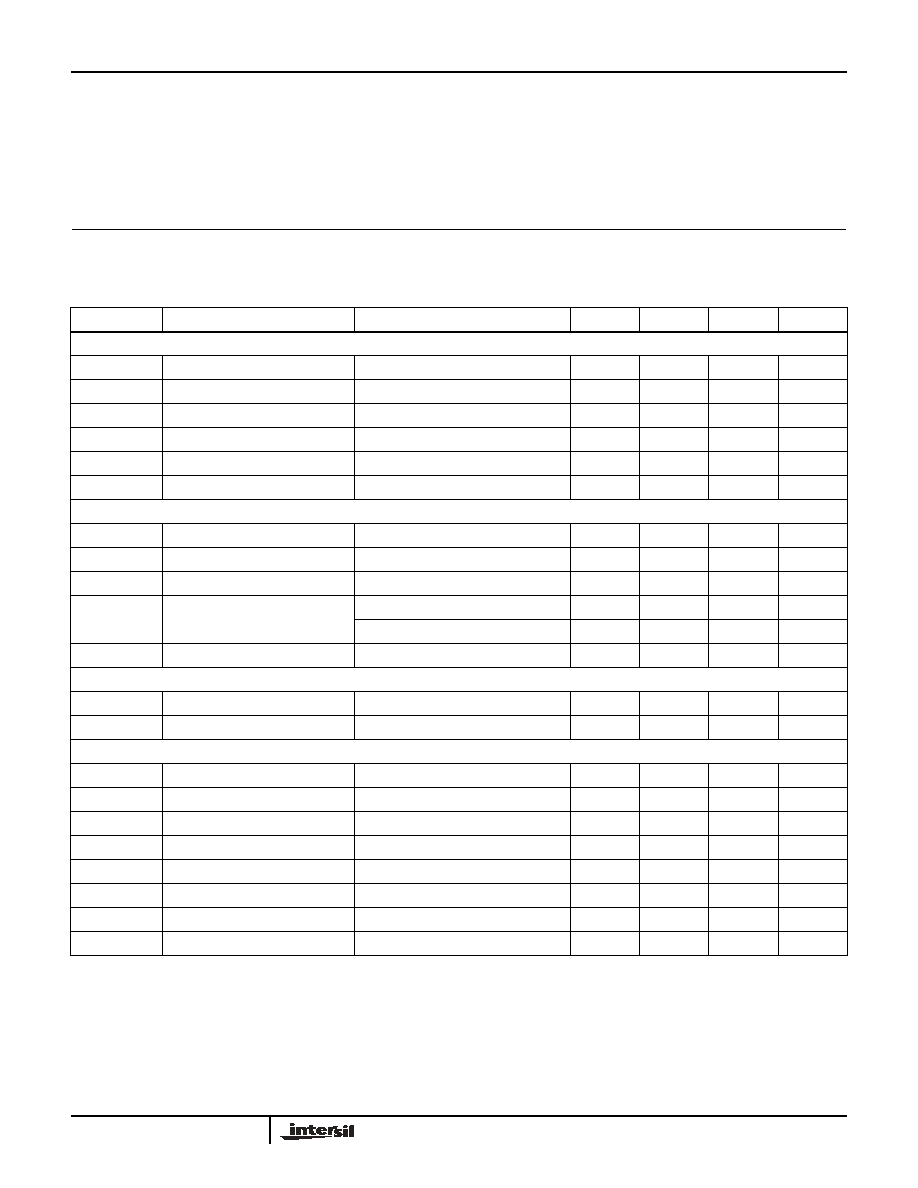
Electrical Specifications
V
S
+ = +15V, V
H
= +15V, V
L
= 0V, T
A
= 25°C, unless otherwise specified.
PARAMETER
DESCRIPTION
CONDITION
MIN
TYP
MAX
UNIT
INPUT
V
IH
Logic `1' Input Voltage
2.4
V
I
IH
Logic `1' Input Current
V
IH
= V
S
+
0.1
10
µA
V
IL
Logic `0' Input Voltage
0.8
V
I
IL
Logic `0' Input Current
V
IL
= 0V
0.1
10
µA
C
IN
Input Capacitance
3.5
pF
R
IN
Input Resistance
50
M
OUTPUT
R
OVH
ON Resistance V
H
to OUT
H
I
OUT
= -200mA
2.7
4.5
R
OVL
ON Resistance V
L
to OUT
L
I
OUT
= +200mA
3.5
5.5
I
OUT
Output Leakage Current
OE = 0V, OUT
H
= V
L
, OUT
L
= V
S
+
0.1
10
µA
I
PK
Peak Output Current
(linear resistive operation)
Source
3.5
A
Sink
3.5
A
I
DC
Continuous Output Current
Source/Sink
200
mA
POWER SUPPLY
I
S
Power Supply Current
Inputs = V
S
+
1.3
3
mA
I
VH
Off Leakage at V
H
V
H
= 0V
4
10
µA
SWITCHING CHARACTERISTICS
t
R
Rise Time
C
L
= 2000pF
14.5
ns
t
F
Fall Time
C
L
= 2000pF
15
ns
t
RF
t
R
, t
F
Mismatch
C
L
= 2000pF
0.5
ns
t
D-1
Turn-Off Delay Time
C
L
= 2000pF
9.5
ns
t
D-2
Turn-On Delay Time
C
L
= 2000pF
10
ns
t
D
t
D-1
-t
D-2
Mismatch
C
L
= 2000pF
0.5
ns
t
D-3
3-state Delay Enable
10
ns
t
D-4
3-state Delay Disable
10
ns
EL7155
3
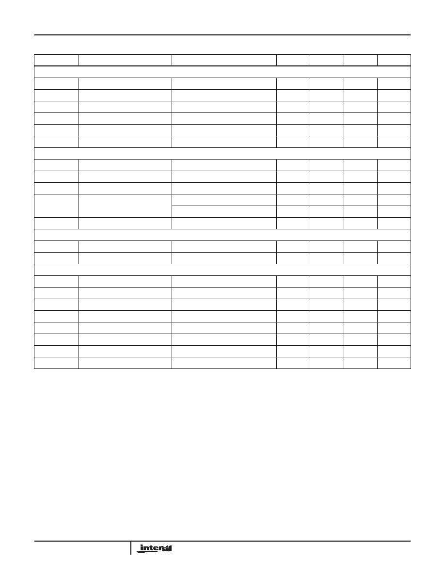
Electrical Specifications
V
S
+ = +5V, V
H
= +5V, V
L
= -5V, T
A
= 25°C, unless otherwise specified.
PARAMETER
DESCRIPTION
CONDITION
MIN
TYP
MAX
UNIT
INPUT
V
IH
Logic `1' Input Voltage
2.0
V
I
IH
Logic `1' Input Current
V
IH
= V
S
+
0.1
10
µA
V
IL
Logic `0' Input Voltage
0.8
V
I
IL
Logic `0' Input Current
V
IL
= 0V
0.1
10
µA
C
IN
Input Capacitance
3.5
pF
R
IN
Input Resistance
50
M
OUTPUT
R
OVH
ON Resistance V
H
to OUT
H
I
OUT
= -200mA
3.4
5
R
OVL
ON Resistance V
L
to OUT
L
I
OUT
= +200mA
4
6
I
OUT
Output Leakage Current
OE = 0V, OUT
H
= V
L
, OUT
L
= V
S
+
0.1
10
µA
I
PK
Peak Output Current
(linear resistive operation)
Source
3.5
A
Sink
3.5
A
I
DC
Continuous Output Current
Source/Sink
200
mA
POWER SUPPLY
I
S
Power Supply Current
Inputs = V
S
+
1
2.5
mA
I
VH
Off Leakage at V
H
V
H
= 0V
4
10
µA
SWITCHING CHARACTERISTICS
t
R
Rise Time
C
L
= 2000pF
17
ns
t
F
Fall Time
C
L
= 2000pF
17
ns
t
RF
t
R
, t
F
Mismatch
C
L
= 2000pF
0
ns
t
D-1
Turn-Off Delay Time
C
L
= 2000pF
11.5
ns
t
D-2
Turn-On Delay Time
C
L
= 2000pF
12
ns
t
D
t
D-1
-t
D-2
Mismatch
C
L
= 2000pF
0.5
ns
t
D-3
3-state Delay Enable
11
ns
t
D-4
3-state Delay Disable
11
ns
EL7155
4
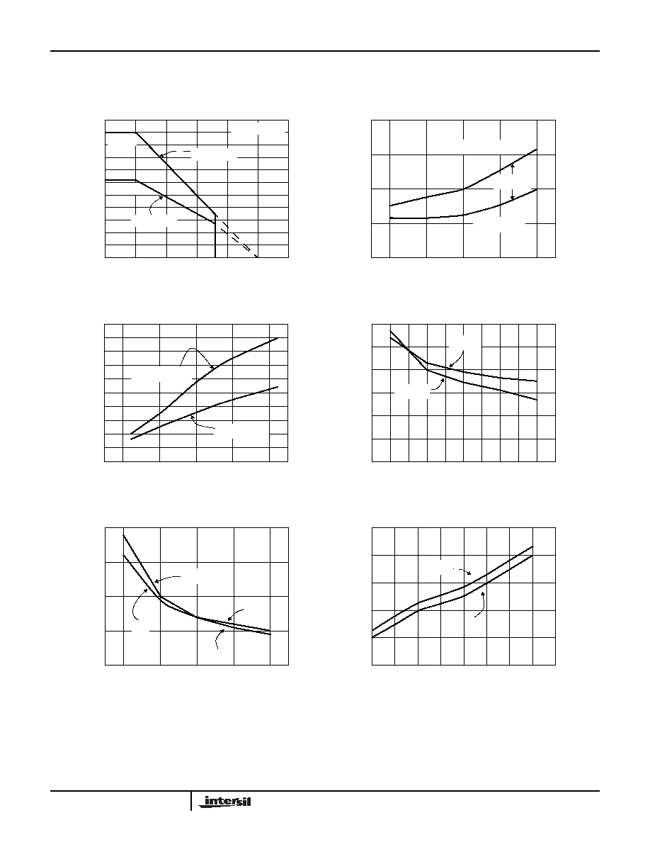
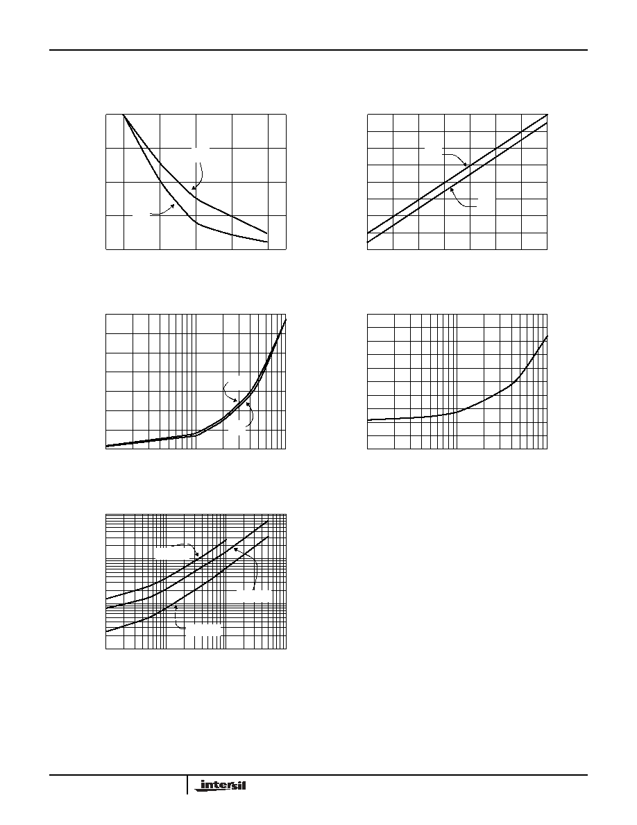
Typical Performance Curves
Input Threshold vs Supply Voltage
T=25°C
1.2
Input
V
o
ltag
e
(V)
Supply Voltage (V)
1.0
1.8
1.6
1.4
15
5
10
High Threshold
Hysteresis
Quiescent Supply Current vs Supply Voltage
T=25°C
15
Suppl
y C
u
r
r
ent
(mA)
Supply Voltage (V)
0
2.0
5
1.6
1.2
0.8
0.4
10
All Inputs = GND
All Inputs = V
S
+
"On" Resistance vs Supply Voltage
I
OUT
=200mA, T=25°C, V
S
+=V
H
, V
L
=0V
Rise/Fall Time vs Supply Voltage
C
L
=2000pF, T=25°C
15
20
R
i
se
/F
al
l Time
(
n
s)
Supply Voltage (V)
10
30
5
Rise/Fall Time vs Temperature
C
L
=2000pF, V
S
+=15V
150
14
R
i
se
/F
al
l Time
(
n
s)
Temperature (°C)
10
100
20
-50
10
25
15
50
16
18
12
0
Low Threshold
t
F
t
R
t
R
t
I
t
R
t
F
"
O
n"
Res
i
st
anc
e
(
)
Supply Voltage (V)
7.5
15
12.5
5
10
1
0
6
5
2
4
3
V
OUT
-V
L
V
OUT
-V
H
Package Power Dissipation vs Ambient Temperature
JEDEC JESD51-3 Low Effective Thermal Conductivity Test Board
P
o
wer D
i
ss
ipation
(W)
Ambient Temperature (°C)
25
100
75
0
50
0.2
1
0.6
0.4
0.8
125
150
0
PDIP8
SO8
Max T
J
=125°C
JA
=100°C/W
JA
=160°C/W
85
EL7155
5
Typical Performance Curves
(Continued)
Propagation Delay vs Supply Voltage
C
L
=2000pF, T=25°C
15
13
D
e
la
y
Time
(ns)
Supply Voltage (V)
9
17
5
Propagation Delay vs Temperature
C
L
=2000pF, V
S
+=15V
D
e
la
y
Time
(ns)
Temperature (°C)
6
14
15
11
10
0
125
-50
50
12
8
-25
25
75
100
1M
10M
10k
100k
0.1
1.0
10
100
Supply Current vs Frequency
C
L
=1000pF, T=25°C
Suppl
y Current
(
m
A)
Frequency (Hz)
10
100
1000
10000
0
1
4
5
3
2
Rise/Fall Time vs Load Capacitance
V
S
+=+15V, T=25°C
10000
30
R
i
se
/F
al
l Time
(
n
s)
Load Capacitance (pF)
0
70
100
Supply Current vs Load Capacitance
V
S
+=V
H
=15V, V
L
=0V, T=25°C, f=20kHz
S
u
ppl
y Cur
r
ent
(
m
A
)
Load Capacitance (pF)
1000
60
50
40
20
10
t
D-2
t
D-1
t
D-2
t
D-1
t
F
t
R
V
S
+=15V
V
S
+=10V
V
S
+=5V
EL7155