1
®
FN7283.1
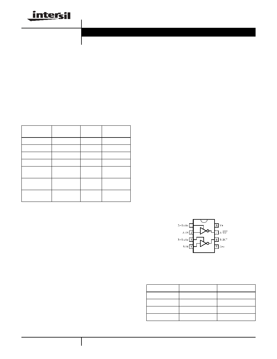
EL7232
Dual Channel, High Speed, High Current
Line Driver w/3-State
The EL7232 3-state drivers are particularly well suited for
ATE and microprocessor based applications. The low
quiescent power dissipation makes this part attractive in
battery applications. The 2A peak drive capability, makes the
EL7232 an excellent choice when driving high speed
capacitive lines, as well. The input circuitry provides level
shifting from TTL levels to the supply rails. The EL7232 is
available in 8-pin PDIP and 8-lead SO packages.
Features
· 3-State output
· 3V and 5V input compatible
· Clocking speeds up to 10MHz
· 20ns Switching/delay time
· 2A Peak drive
· Low, matched output impedance--5
· Low quiescent current -- 2.5mA
· Wide operating voltage -- 4.5V-16V
·
Pb-Free available (RoHS compliant)
Applications
· Parallel bus line drivers
· EPROM and PROM programming
· Motor controls
· Charge pumps
· Sampling circuits
· Pin drivers
· Bridge circuits
Pinout
Ordering Information
PART NUMBER
PACKAGE
TAPE &
REEL
PKG. DWG. #
EL7232CN
8-Pin PDIP
-
MDP0031
EL7232CS
8-Pin SO
-
MDP0027
EL7232CS-T7
8-Pin SO
7"
MDP0027
EL7232CS-T13
8-Pin SO
13"
MDP0027
EL7232CSZ
(See Note)
8-Pin SO
(Pb-free)
-
MDP0027
EL7232CSZ-T7
(See Note)
8-Pin SO
(Pb-free)
7"
MDP0027
EL7232CSZ-T13
(See Note)
8-Pin SO
(Pb-free)
13"
MDP0027
NOTE: Intersil Pb-free products employ special Pb-free material sets;
molding compounds/die attach materials and 100% matte tin plate
termination finish, which are RoHS compliant and compatible with
both SnPb and Pb-free soldering operations. Intersil Pb-free products
are MSL classified at Pb-free peak reflow temperatures that meet or
exceed the Pb-free requirements of IPC/JEDEC J STD-020.
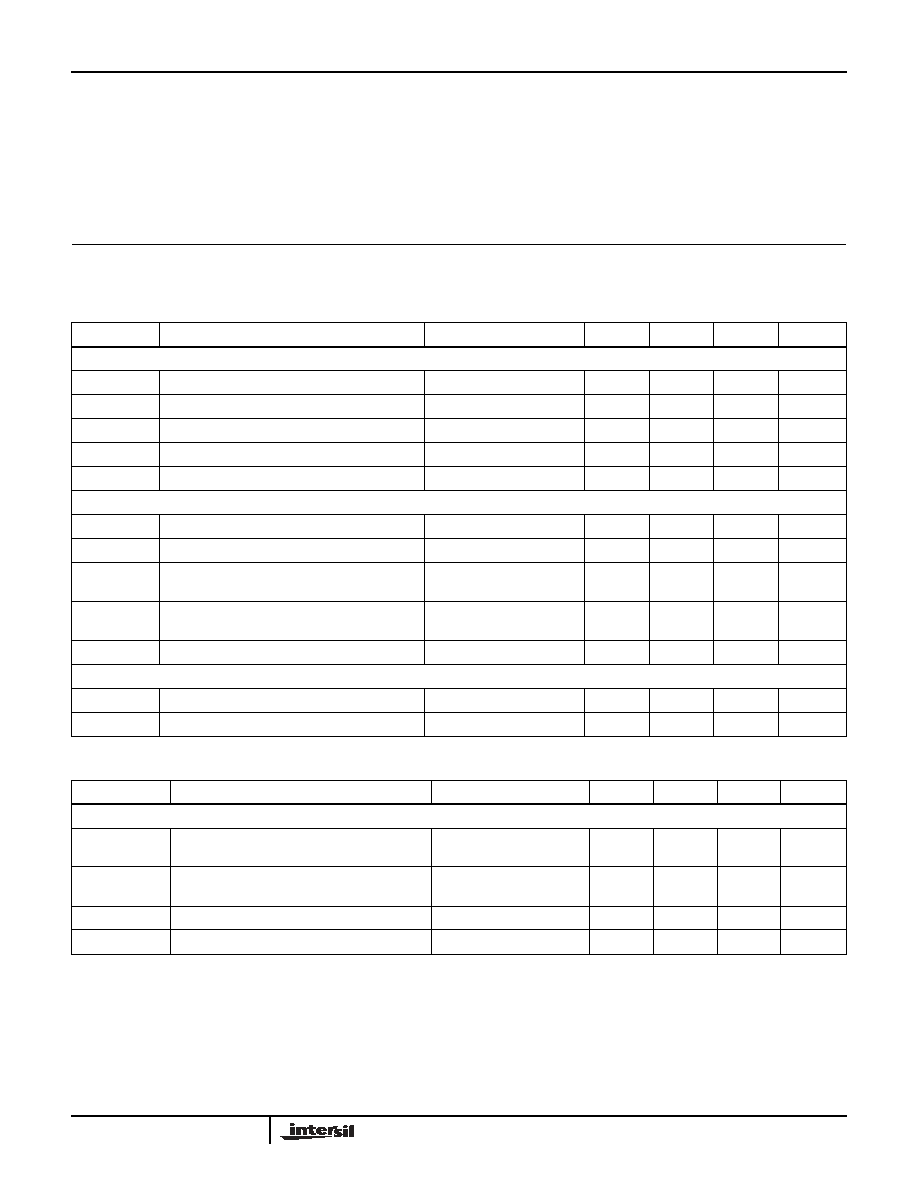
Truth Table
3-STATE
INPUT
OUTPUT
1
0
1
1
1
0
0
0
Open
0
1
Open
Manufactured under U.S. Patent Nos. 5,334,883, #5,341,047
EL7232
(8-PIN PDIP, SO)
TOP VIEW
Data Sheet
April 11, 2005
CAUTION: These devices are sensitive to electrostatic discharge; follow proper IC Handling Procedures.
1-888-INTERSIL or 1-888-352-6832
|
Intersil (and design) is a registered trademark of Intersil Americas Inc.
Copyright Intersil Americas Inc. 2003, 2005. All Rights Reserved
All other trademarks mentioned are the property of their respective owners.
2
Absolute Maximum Ratings
(T
A
= 25°C)
Supply (V+ to Gnd) . . . . . . . . . . . . . . . . . . . . . . . . . . . . . . . . . 16.5V
Input Pins . . . . . . . . . . . . . . . . . . . . . . . . . . -0.3V to +0.3V above V+
Combined Peak Output Current. . . . . . . . . . . . . . . . . . . . . . . . . . .4A
Storage Temperature Range . . . . . . . . . . . . . . . . . .-65°C to +150°C
Ambient Operating Temperature . . . . . . . . . . . . . . . .-40°C to +85°C
Operating Junction Temperature . . . . . . . . . . . . . . . . . . . . . . . 125°C
Power Dissipation
SOIC . . . . . . . . . . . . . . . . . . . . . . . . . . . . . . . . . . . . . . 570mW
PDIP . . . . . . . . . . . . . . . . . . . . . . . . . . . . . . . . . . . . . 1050mW
CAUTION: Stresses above those listed in "Absolute Maximum Ratings" may cause permanent damage to the device. This is a stress only rating and operation of the
device at these or any other conditions above those indicated in the operational sections of this specification is not implied.
IMPORTANT NOTE: All parameters having Min/Max specifications are guaranteed. Typical values are for information purposes only. Unless otherwise noted, all tests
are at the specified temperature and are pulsed tests, therefore: T
J
= T
C
= T
A
DC Electrical Specifications
T
A
= 25°C, V = 15V unless otherwise specified
PARAMETER
DESCRIPTION
TEST CONDITIONS
MIN
TYP
MAX
UNITS
INPUT
V
IH
Logic "1" Input Voltage
2.4
V
I
IH
Logic "1" Input Current
@V+
0.1
10
µA
V
IL
Logic "0" Input Voltage
0.8
V
I
IL
Logic "0" Input Current
@0V
0.1
10
µA
V
HVS
Input Hysteresis
0.3
V
OUTPUT
R
OH
Pull-Up Resistance
I
OUT
= -100 mA
3
6
R
OL
Pull-Down Resistance
I
OUT
= +100 mA
4
6
I
OFF
3-State Output Leakage
V
OUT
= V+
V
OUT
= 0V
0.2
10
µA
I
PK
Peak Output Current
Source
Sink
2.0
2.0
A
I
DC
Continuous Output Current
Source/Sink
100
mA
POWER SUPPLY
I
S
Power Supply Current
Inputs High
1
2.5
mA
V
S
Operating Voltage
4.5
16
V
AC Electrical Specifications
T
A
= 25°C, V = 15V unless otherwise specified
PARAMETER
DESCRIPTION
TEST CONDITIONS
MIN
TYP
MAX
UNITS
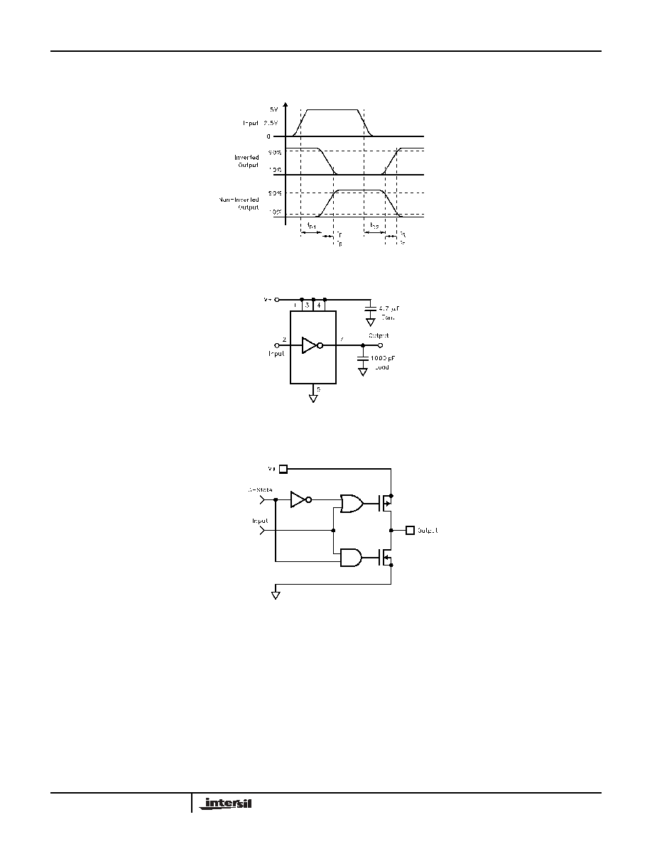
SWITCHING CHARACTERISTICS
t
R
Rise Time
C
L
= 500pF
C
L
= 1000pF
7.5
10
ns
t
F
Fall Time
C
L
= 500pF
C
L
= 1000pF
10
13
20
ns
t
D-ON
Turn-On Delay Time
18
25
ns
t
D-OFF
Turn-Off Delay Time
20
25
ns
EL7232
4
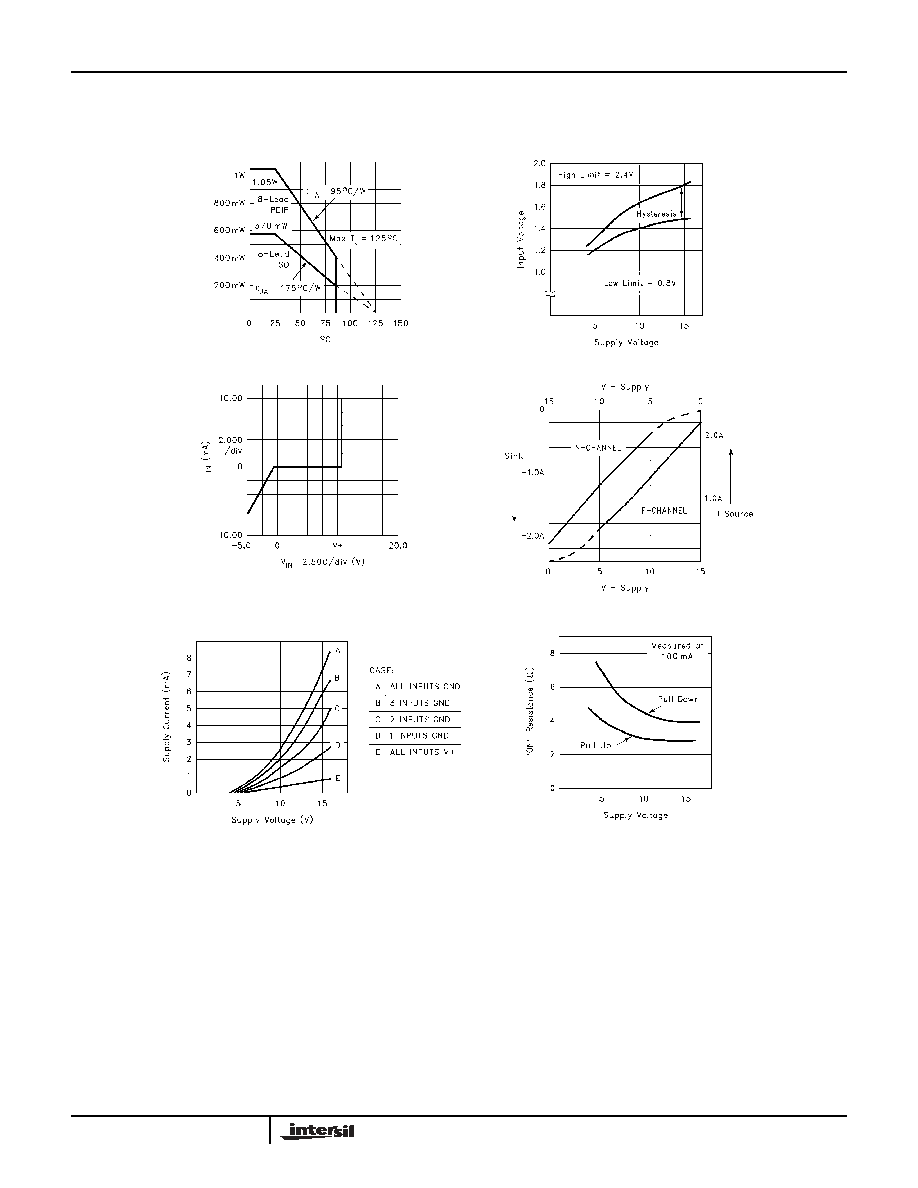
Typical Performance Curves
Switch Threshold vs Supply Voltage
Max Power/Derating Curves
Input Current vs Voltage
Peak Drive vs Supply Voltage
Quiescent Supply Current
"ON" Resistance vs Supply Voltage
EL7232
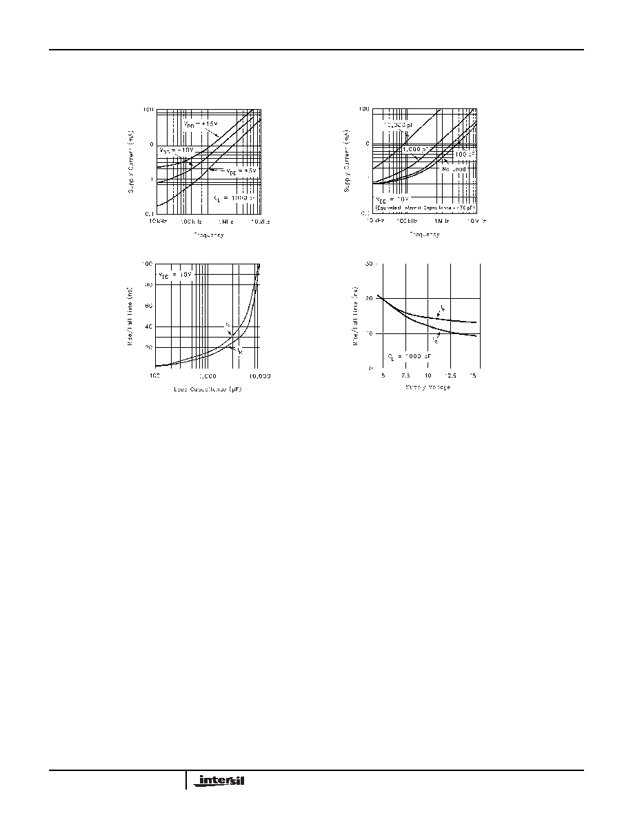
5
Typical Performance Curves
(Continued)
Average Supply Current vs
Voltage and Frequency
Average Supply Current
vs Capacitive Load
Rise/Fall Time vs Load
Rise/Fall Time vs Supply Voltage
EL7232