1
®
FN7286.1
EL7243
Dual Input, High Speed, Dual Channel
CCD Driver
The EL7243 dual input, 2-channel driver achieves the same
excellent switching performance of the EL7212 family while
providing added flexibility. The power package makes this
part extremely well suited for high frequency and heavy
loads as in CCD applications. The 2-input logic and
configuration is applicable to numerous power MOSFET
drive circuits. As with other Elantec drivers, the EL7243 is
excellent for driving large capacitive loads with minimal delay
and switching times. "Shoot-thru" protection and latching
circuits can be implemented by simply "cross-coupling" the
2-channels.
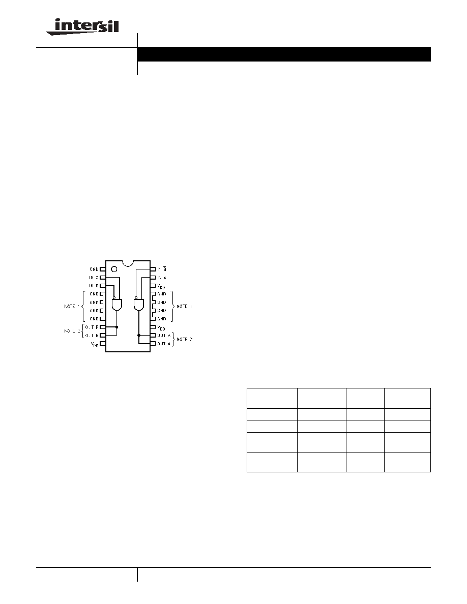
Pinout
EL7243
(20-PIN THERMAL SOIC)
TOP VIEW
Features
· Logic AND/NAND input
· 3V and 5V Input compatible
· Clocking speeds up to 20MHz
· 20ns Switching/delay time
· 2A Peak drive
· Isolated drains
· Low output impedance
· Low quiescent current
· Wide operating voltage -- 4.5V to 16V
·
Pb-Free available (RoHS compliant)
Applications
· CCD Drivers
· Short circuit protected switching
· Under-voltage shut-down circuits
· Switch-mode power supplies
· Motor controls
· Power MOSFET switching
· Switching capacitive loads
· Shoot-thru protection
· Latching drivers
Note 1: Pins 47 and 1417 are electrically connected.
Note 2: Output pins must be tied together.
Manufactured under U.S. Patent Nos. 5,334,883, #5,341,047
Ordering Information
PART NUMBER
PACKAGE
TAPE &
REEL
PKG. DWG. #
EL7243CM
20-Pin SOIC
-
MDP0027
EL7243CM-T13
20-Pin SOIC
13"
MDP0027
EL7243CMZ
(See Note)
20-Pin SOIC
(Pb-free)
-
MDP0027
EL7243CMZ-T13
(See Note)
20-Pin SOIC
(Pb-free)
13"
MDP0027
NOTE: Intersil Pb-free products employ special Pb-free material sets;
molding compounds/die attach materials and 100% matte tin plate
termination finish, which are RoHS compliant and compatible with
both SnPb and Pb-free soldering operations. Intersil Pb-free products
are MSL classified at Pb-free peak reflow temperatures that meet or
exceed the Pb-free requirements of IPC/JEDEC J STD-020.
Data Sheet
May 13, 2005
CAUTION: These devices are sensitive to electrostatic discharge; follow proper IC Handling Procedures.
1-888-INTERSIL or 1-888-352-6832
|
Intersil (and design) is a registered trademark of Intersil Americas Inc.
Copyright Intersil Americas Inc. 1996, 2003, 2005. All Rights Reserved
All other trademarks mentioned are the property of their respective owners.
2
Absolute Maximum Ratings
(T
A
= 25°C)
Supply (V+ to Gnd) . . . . . . . . . . . . . . . . . . . . . . . . . . . . . . . . . 16.5V
Input Pins . . . . . . . . . . . . . . . . . . . . . . . . . . -0.3V to +0.3V above V+
Combined Peak Output Current. . . . . . . . . . . . . . . . . . . . . . . . . . .4A
Storage Temperature Range . . . . . . . . . . . . . . . . . .-65°C to +150°C
Ambient Operating Temperature . . . . . . . . . . . . . . . . -40°C to +85°C
Operating Junction Temperature . . . . . . . . . . . . . . . . . . . . . . . 125°C
Power Dissipation
20-pin "Batwing" SOIC . . . . . . . . . . . . . . . . . . . . . . . 1500mW
CAUTION: Stresses above those listed in "Absolute Maximum Ratings" may cause permanent damage to the device. This is a stress only rating and operation of the
device at these or any other conditions above those indicated in the operational sections of this specification is not implied.
IMPORTANT NOTE: All parameters having Min/Max specifications are guaranteed. Typical values are for information purposes only. Unless otherwise noted, all tests
are at the specified temperature and are pulsed tests, therefore: T
J
= T
C
= T
A
DC Electrical Specifications
T
A
= 25°C, V
DD
= 15V unless otherwise specified
PARAMETER
DESCRIPTION
TEST CONDITIONS
MIN
TYP
MAX
UNITS
INPUT
V
IH
Logic "1" Input Voltage
2.4
V
I
IH
Logic "1" Input Current
@V
DD
0.1
10
µA
V
IL
Logic "0" Input Voltage
0.8
V
I
IL
Logic "0" Input Current
@0V
0.1
10
µA
V
HVS
Input Hysteresis
0.3
V
OUTPUT
R
OH
Pull-Up Resistance
I
OUT
= -100mA
3
6
R
OL
Pull-Down Resistance
I
OUT
= +100mA
4
6
I
PK
Peak Output Current
Source
Sink
2
2
A
I
DC
Continuous Output Current
Source/Sink
200
mA
POWER SUPPLY
I
S
Power Supply Current
Inputs High
1
2.5
mA
V
S
Operating Voltage
4.5
16
V
AC Electrical Specifications
T
A
= 25°C, V = 15V unless otherwise specified
PARAMETER
DESCRIPTION
TEST CONDITIONS
MIN
TYP
MAX
UNITS
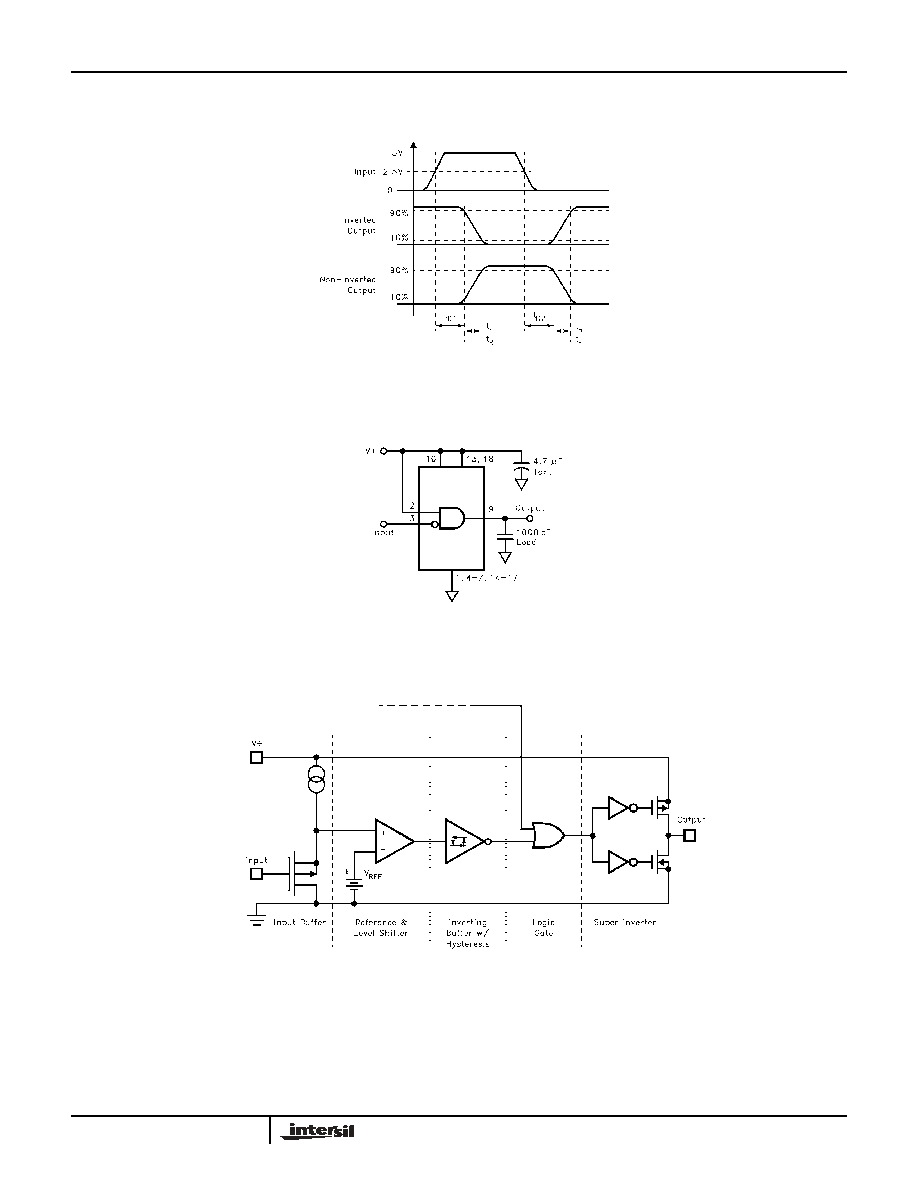
SWITCHING CHARACTERISTICS
t
R
Rise Time
C
L
= 500pF
C
L
= 1000pF
10
20
ns
t
F
Fall Time
C
L
= 500pF
C
L
= 1000pF
10
20
ns
t
D-ON
Turn-On Delay Time
20
25
ns
t
D-OFF
Turn-Off Delay Time
20
25
ns
EL7243
4
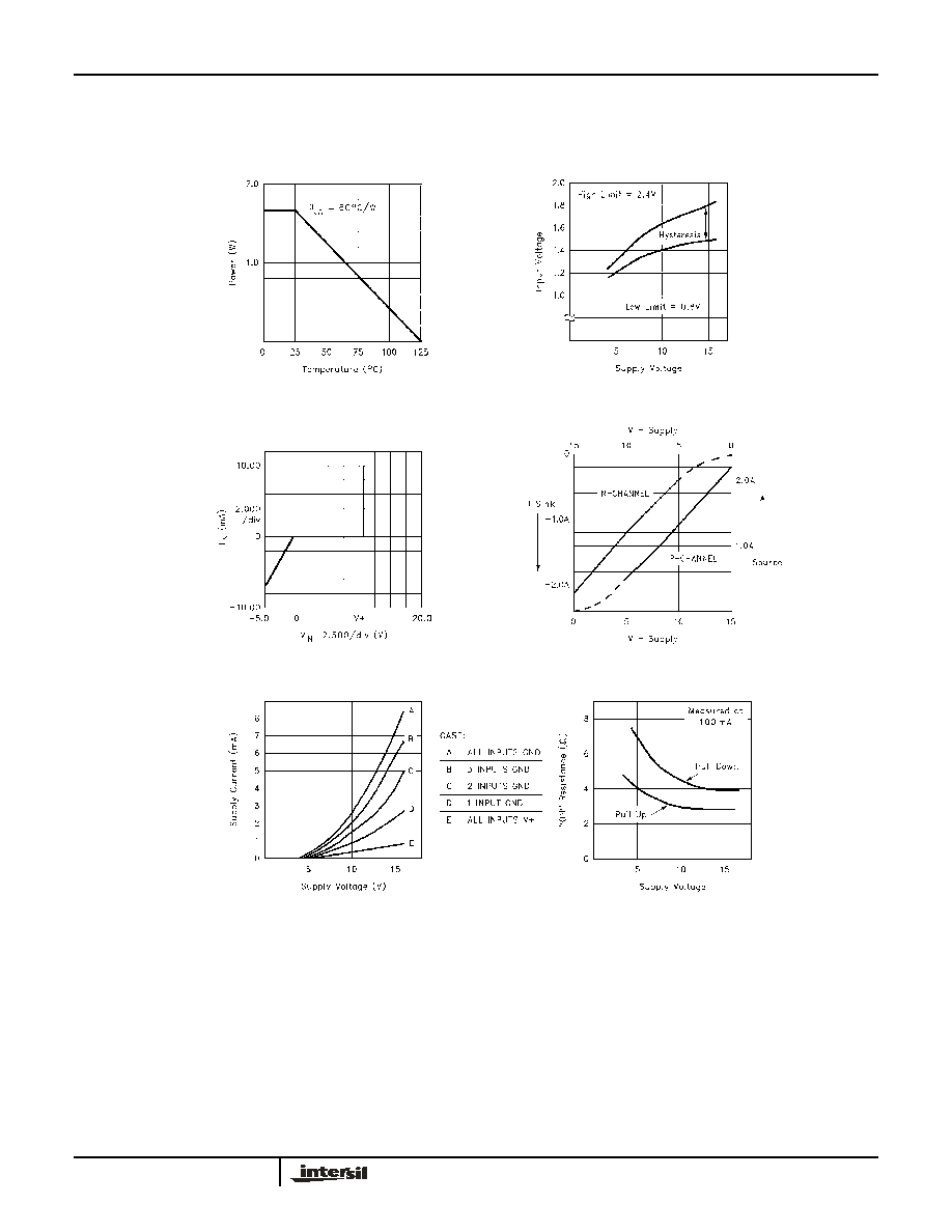
Typical Performance Curves
Max Power/Derating Curves
Switch Threshold vs Supply Voltage
Input Current vs Voltage
Quiescent Supply Current
"ON" Resistance vs Supply Voltage
Peak Drive vs Supply Voltage
EL7243
5
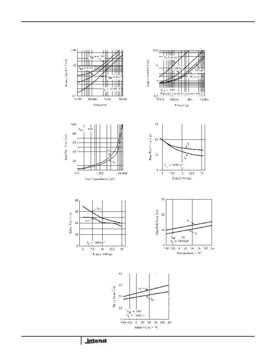
Typical Performance Curves
(Continued)
Average Supply Current vs
Voltage and Frequency
Average Supply Current
vs Capacitive Load
Rise/Fall Time vs Load
Rise/Fall Time vs Supply Voltage
Rise/Fall Time vs Temperature
Propagation Delay vs Supply Voltage
Delay vs Temperature
EL7243