1
Æ
FN7120.1
EL7515
High Frequency PWM Step-Up Regulator
The EL7515 is a high frequency, high efficiency step-up
DC:DC regulator operated at fixed frequency PWM mode.
With an integrated 1.4A MOSFET, it can deliver up to 600mA
output current at up to 92% efficiency. The adjustable
switching frequency is up to 1.2MHz, making it ideal for DSL
applications.
When shut down, it draws <1µA of current. This feature,
along with the minimum starting voltage of 1.8V, makes it
suitable for portable equipment powered by one lithium ion,
3 to 4 NiMH cells, or 2 cells of alkaline battery.
The EL7515 is available in a 10-pin MSOP package, with
maximum height of 1.1mm. With proper external
components, the whole converter takes less than 0.25in
2
PCB space.
This device is specified for operation over the full -40∞C to
+85∞C temperature range.
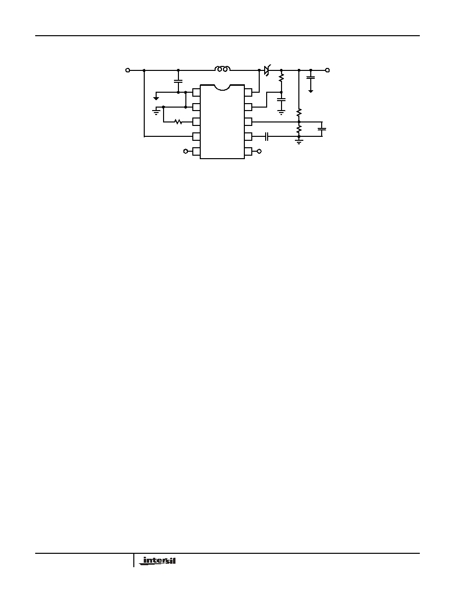
Pinout
EL7515
(10-PIN MSOP)
TOP VIEW
Features
∑ Up to 92% efficiency
∑ Up to 600mA I
OUT
∑ 4.5V < V
OUT
< 17V
∑ 1.8V < V
IN
< 13.2V
∑ Up to 1.2MHz adjustable frequency
∑ <1µA shutdown current
∑ Adjustable soft-start
∑ Low battery detection
∑ Internal thermal protection
∑ 1.1mm max height 10-pin MSOP package
∑ Pb-Free available (RoHS compliant)
Applications
∑ 3V to 5V and 12V converters
∑ 5V to 12V converters
∑ TFT-LCD
∑ DSL
∑ Portable equipment
∑ Desktop equipment
LX
VDD
FB
SS
LBO
LBI
EN
SGND
RT
PGND 1
2
3
4
10
9
8
7
5
6
Ordering Information
PART
NUMBER
PACKAGE
TAPE & REEL PKG. DWG. #
EL7515IY
10-Pin MSOP
-
MDP0043
EL7515IY-T7
10-Pin MSOP
7"
MDP0043
EL7515IY-T13
10-Pin MSOP
13"
MDP0043
EL7515IYZ
(See Note)
10-Pin MSOP
(Pb-free)
-
MDP0043
EL7515IYZ-T7
(See Note)
10-Pin MSOP
(Pb-free)
7"
MDP0043
EL7515IYZ-
T13 (See Note)
10-Pin MSOP
(Pb-free)
13"
MDP0043
NOTE: Intersil Pb-free products employ special Pb-free material sets;
molding compounds/die attach materials and 100% matte tin plate
termination finish, which are RoHS compliant and compatible with
both SnPb and Pb-free soldering operations. Intersil Pb-free products
are MSL classified at Pb-free peak reflow temperatures that meet or
exceed the Pb-free requirements of IPC/JEDEC J STD-020.
Data Sheet
May 13, 2005
CAUTION: These devices are sensitive to electrostatic discharge; follow proper IC Handling Procedures.
1-888-INTERSIL or 1-888-352-6832
|
Intersil (and design) is a registered trademark of Intersil Americas Inc.
Copyright Intersil Americas Inc. 2003, 2005. All Rights Reserved
All other trademarks mentioned are the property of their respective owners.
3
FN7120.1
May 13, 2005
IMPORTANT NOTE: All parameters having Min/Max specifications are guaranteed. Typ values are for information purposes only. Unless otherwise noted, all tests are
at the specified temperature and are pulsed tests, therefore: T
J
= T
C
= T
A
Absolute Maximum Ratings
(T
A
= 25∞C)
EN, LBI, V
DD
. . . . . . . . . . . . . . . . . . . . . . . . . . . . . . . . . . . . . . .+12V
LX . . . . . . . . . . . . . . . . . . . . . . . . . . . . . . . . . . . . . . . . . . . . . . .+18V
Storage Temperature . . . . . . . . . . . . . . . . . . . . . . . .-65∞C to +150∞C
Operating Temperature . . . . . . . . . . . . . . . . . . . . . . .-40∞C to +85∞C
Operating Junction Temperature: . . . . . . . . . . . . . . . . . . . . . . 135∞C
CAUTION: Stresses above those listed in "Absolute Maximum Ratings" may cause permanent damage to the device. This is a stress only rating and operation of the
device at these or any other conditions above those indicated in the operational sections of this specification is not implied.
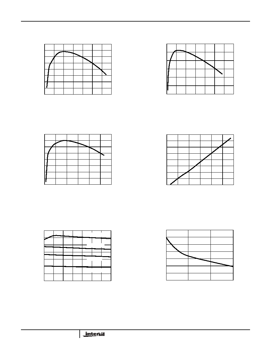
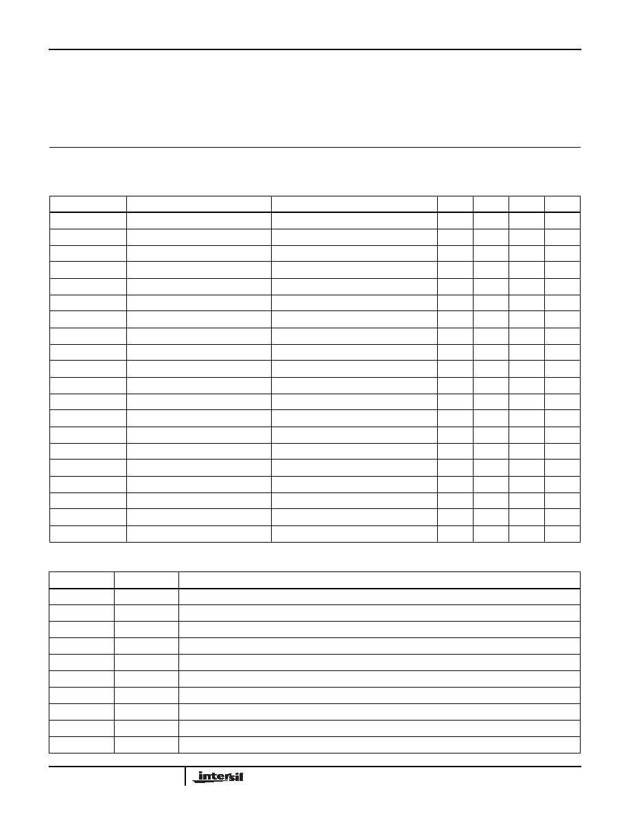
Electrical Specifications
V
IN
= 5V, V
OUT
= 12V, L = 10µH, I
OUT
= 0mA, R
T
= 100k
, T
A
= 25∞C, Unless Otherwise Specified.
PARAMETER
DESCRIPTION
CONDITIONS
MIN
TYP
MAX
UNIT
V
IN
Input Voltage Range
1.8
13.2
V
V
OUT
Output Voltage Range
4.5
17
V
IQ1
Quiescent Current - Shut-down
V
EN
= 0, feedback resisters disconnected
1
µA
IQ2
Quiescent Current
V
EN
= 2V
1.4
2
mA
V
FB
Feedback Voltage
1.29
1.33
1.37
V
IB
Feedback Input Bias Current
0.10
µA
D
MAX
Maximum Duty Cycle
84
90
%
I
LIM
Current Limit - Max Peak Input Current
1
1.4
A
I
SHDN
Shut-down Input Bias Current
1
µA
V
LBI
LBI Threshold Voltage
180
220
250
mV
V
OL-LBO
LBO Output Low
I
LBO
= 1mA
0.1
0.2
V
I
LEAK-LBO
LBO Output Leakage Current
V
LBI
= 250mV, V
LBO
= 5V
0.02
2
µA
R
DS-ON
Switch On Resistance
at 12V output
220
m
I
LEAK-SWITCH
Switch Leakage Current
1
µA
V
OUT
/
V
IN
/V
OUT
Line Regulation
3V < V
IN
< 6V, V
OUT
= 12V, no load
0.4
%/V
V
OUT
/V
OUT
Load Regulation
I
OUT
= 50mA to 150mA
1
%
F
OSC-MAX
Maximum Switching Frequency
R
T
= 49.9k
1200
kHz
F
OSC1
Switching Frequency
600
670
750
kHz
VHI_EN
EN Input High Threshold
1.6
V
VLO_EN
EN Input Low Threshold
0.5
V
Pin Descriptions
PIN NUMBER
PIN NAME
PIN FUNCTION
1
PGND
Power ground; connected to the source of internal N-channel power MOSFET
2
SGND
Signal ground; ground reference for all the control circuitry; needs to have only a single connection to PGND
3
RT
Timing resistor to adjust the oscillation frequency of the converter
4
EN
Chip enable; connects to logic HI (>1.6V) for chip to function
5
LBI
Low battery input; connects to a sensing voltage, or left open if function is not used
6
LBO
Low battery detection output; connected to the open drain of a MOSFET; able to sink 1mA current
7
SS
Soft-start; connects to a capacitor to control the start-up of the converter
8
FB
Voltage feedback input; needs to connect to resistor divider to decide V
O
9
VDD
Control circuit positive supply
10
LX
Inductor drive pin; connected to the drain of internal N-channel power MOSFET
EL7515