 | –≠–ª–µ–∫—Ç—Ä–æ–Ω–Ω—ã–π –∫–æ–º–ø–æ–Ω–µ–Ω—Ç: EL7516IYZ | –°–∫–∞—á–∞—Ç—å:  PDF PDF  ZIP ZIP |
1
Æ
FN7333.4
EL7516
600kHz/1.2MHz PWM Step-Up Regulator
The EL7516 is a high frequency, high efficiency step-up
voltage regulator operated at constant frequency PWM
mode. With an internal 1.5A, 200m
MOSFET, it can deliver
up to 600mA output current at over 90% efficiency. The
selectable 600kHz and 1.2MHz allows smaller inductors and
faster transient response. An external compensation pin
gives the user greater flexibility in setting frequency
compensation allowing the use of low ESR Ceramic output
capacitors.
When shut down, it draws < 10µA of current and can operate
down to 2.5V input supply. These features along with
1.2MHz switching frequency makes it an ideal device for
portable equipment and TFT-LCD displays.
The EL7516 is available in an 8-pin MSOP package with a
maximum height of 1.1mm. The device is specified for
operation over the full -40∞C to +85∞C temperature range.
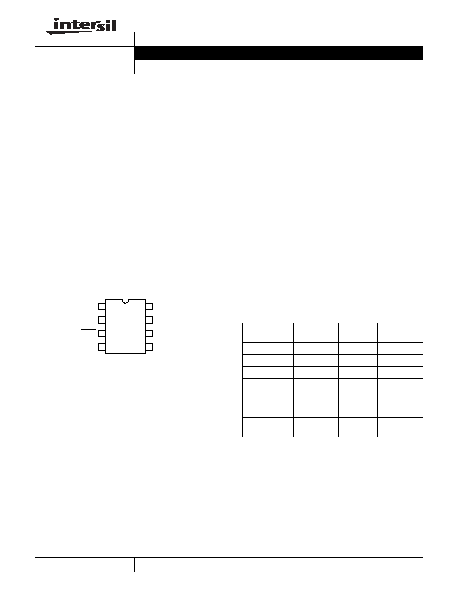
Pinout
EL7516
(8-PIN MSOP)
TOP VIEW
Features
∑ >90% efficiency
∑ 1.6A, 200m
power MOSFET
∑ V
IN
> 2.5V
∑ 600kHz/1.2MHz switching frequency selection
∑ Adjustable soft-start
∑ Internal thermal protection
∑ 1.1mm max height 8-pin MSOP package
∑ Pb-free available (RoHS compliant)
Applications
∑ TFT-LCD displays
∑ DSL modems
∑ PCMCIA cards
∑ Digital cameras
∑ GSM/CDMA phones
∑ Portable equipment
∑ Handheld devices
FB
FSEL
SHDN
VDD
GND
LX
COMP
SS
1
2
3
4
8
7
6
5
Ordering Information
PART NUMBER
PACKAGE
TAPE &
REEL
PKG. DWG. #
EL7516IY
8-Pin MSOP
-
MDP0043
EL7516IY-T7
8-Pin MSOP
7"
MDP0043
EL7516IY-T13
8-Pin MSOP
13"
MDP0043
EL7516IYZ
(See Note)
8-Pin MSOP
(Pb-Free)
-
MDP0043
EL7516IYZ-T7
(See Note)
8-Pin MSOP
(Pb-Free)
7"
MDP0043
EL7516IYZ-T13
(See Note)
8-Pin MSOP
(Pb-Free)
13"
MDP0043
NOTE: Intersil Pb-free products employ special Pb-free material sets;
molding compounds/die attach materials and 100% matte tin plate
termination finish, which are RoHS compliant and compatible with
both SnPb and Pb-free soldering operations. Intersil Pb-free products
are MSL classified at Pb-free peak reflow temperatures that meet or
exceed the Pb-free requirements of IPC/JEDEC J STD-020.
Data Sheet
March 4, 2005
CAUTION: These devices are sensitive to electrostatic discharge; follow proper IC Handling Procedures.
1-888-INTERSIL or 1-888-352-6832
|
Intersil (and design) is a registered trademark of Intersil Americas Inc.
Copyright Intersil Americas Inc. 2002, 2004, 2005. All Rights Reserved
All other trademarks mentioned are the property of their respective owners.
2
FN7333.4
March 4, 2005
Absolute Maximum Ratings
(T
A
= 25∞C)
LX to GND . . . . . . . . . . . . . . . . . . . . . . . . . . . . . . . . . . . . . . . . . .18V
V
DD
to GND. . . . . . . . . . . . . . . . . . . . . . . . . . . . . . . . . . . . . . . . . .6V
COMP, FB, SHDN, SS, FSEL to GND . . . . . . . -0.3V to (V
DD
+0.3V)
Storage Temperature . . . . . . . . . . . . . . . . . . . . . . . .-65∞C to +150∞C
Operating Ambient Temperature . . . . . . . . . . . . . . . .-40∞C to +85∞C
Operating Junction Temperature . . . . . . . . . . . . . . . . . . . . . . +135∞C
CAUTION: Stresses above those listed in "Absolute Maximum Ratings" may cause permanent damage to the device. This is a stress only rating and operation of the
device at these or any other conditions above those indicated in the operational sections of this specification is not implied.
IMPORTANT NOTE: All parameters having Min/Max specifications are guaranteed. Typical values are for information purposes only. Unless otherwise noted, all tests
are at the specified temperature and are pulsed tests, therefore: T
J
= T
C
= T
A
Electrical Specifications
V
IN
= 3.3V, V
OUT
= 12V, I
OUT
= 0mA, FSEL = GND, T
A
= 25∞C unless otherwise specified.
PARAMETER
DESCRIPTION
CONDITIONS
MIN
TYP
MAX
UNIT
IQ1
Quiescent Current - Shut-down
SHDN = 0V
0.6
10
µA
IQ2
Quiescent Current - Not Switching
SHDN = V
DD
, FB = 1.3V
0.7
mA
IQ3
Quiescent Current - Switching
SHDN = V
DD
, FB = 1.0V
1.3
2
mA
V
FB
Feedback Voltage
1.272
1.294
1.309
V
I
B-FB
Feedback Input Bias Current
0.01
0.5
µA
V
DD
Start-Up Input Voltage Range
2.6
5.5
V
D
MAX
-600kHz
Maximum Duty Cycle
FSEL = 0V
84
90
%
D
MAX
-1.2MHz Maximum Duty Cycle
FSEL = V
DD
84
90
%
I
LIM
Current Limit - Max Peak Input Current
1.3
1.5
A
I
SHDN
Shut-down Input Bias Current
SHDN = 0V
0.01
0.1
µA
R
DS-ON
Switch ON Resistance
V
DD
= 2.7V, I
LX
= 1A
0.2
I
LX-LEAK
Switch Leakage Current
VSW = 18V
0.01
3
µA
V
OUT
/
V
IN
Line Regulation
3V < V
IN
< 5.5V, V
OUT
= 12V
0.1
%
V
OUT
/
I
OUT
Load Regulation
V
IN
= 3.3V, V
OUT
= 12V, I
O
= 30mA to 200mA
6.7
mV/A
F
OSC1
Switching Frequency Accuracy
FSEL = 0V
500
620
740
kHz
F
OSC2
Switching Frequency Accuracy
FSEL = V
DD
1000
1250
1500
kHz
V
IL
SHDN, FSEL Input Low Level
0.5
V
V
IH
SHDN, FSEL Input High Level
2.7
V
V
IL
SHDN, Input Low Level
5V Input Supply
1.25
V
V
IH
SHDN, Input High Level
5V Input Supply
4.5
V
G
M
Error Amp Tranconductance
I = 5µA
90
130
170
1µ/
A
V
Voltage Gain
350
V/V
V
DD-ON
V
DD
UVLO On Threshold
2.40
2.51
2.60
V
V
DD-OFF
V
DD
UVLO Off Threshold
2.20
2.30
2.40
V
I
SS
Soft-start Charge Current
4
6
8
µA
R
CS
Current Sense Transresistance
0.08
V/A
OTP
Over Temperature Protection
130
∞C
EL7516
3
FN7333.4
March 4, 2005
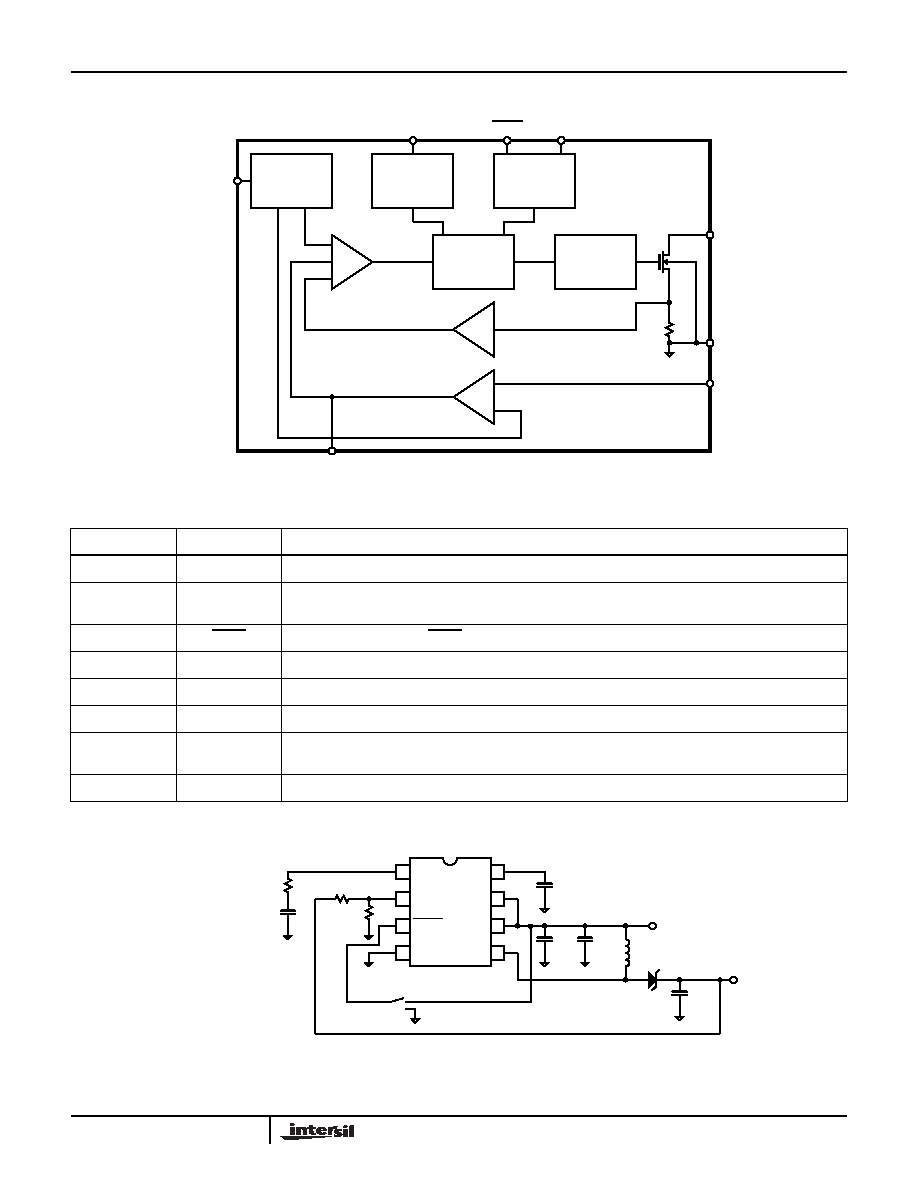
Block Diagram
Typical Application Circuit
COMPARATOR
OSCILLATOR
SHUTDOWN &
START-UP
CONTROL
LX
VDD
FSEL
SHDN
SS
REFERENCE
GENERATOR
PWM LOGIC
CONTROLLER
FET
DRIVER
CURRENT
SENSE
GM
AMPLIFIER
GND
FB
COMP
Pin Descriptions
PIN NUMBER
PIN NAME
DESCRIPTION
1
COMP
Compensation pin. Output of the internal error amplifier. Capacitor and resistor from COMP pin to ground.
2
FB
Voltage feedback pin. Internal reference is 1.294V nominal. Connect a resistor divider from V
OUT
. V
OUT
=
1.294V (1 + R
1
/ R
2
). See Typical Application Circuit.
3
SHDN
Shutdown control pin. Pull SHDN low to turn off the device.
4
GND
Analog and power ground.
5
LX
Power switch pin. Connected to the drain of the internal power MOSFET.
6
VDD
Analog power supply input pin.
7
FSEL
Frequency select pin. When FSEL is set low, switching frequency is set to 620kHz. When connected to
high or V
DD
, switching frequency is set to 1.25MHz.
8
SS
Soft-start control pin. Connect a capacitor to control the converter start-up.
1
2
3
4
8
7
6
5
COMP
FB
SHDN
GND
SS
FSEL
VDD
LX
+
+
3.9k
4.7nF
27nF
22µF
C
3
C
1
0.1µF
10µH
D
1
22µF
C
2
12V
2.7V TO 5.5V
R
3
C
5
85.2k
R
1
10k
R
2
C
4
S1
EL7516

4
FN7333.4
March 4, 2005
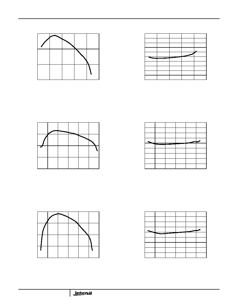
Typical Performance Curves
FIGURE 1. EFFICIENCY - 3.3V V
IN
TO 12V V
OUT
@ 1.3MHz
FIGURE 2. LOAD REGULATION - 3.3V V
IN
TO 12V V
OUT
@ 1.3MHz
FIGURE 3. EFFICIENCY - 3.3V V
IN
TO 12V V
OUT
@ 620kHz
FIGURE 4. LOAD REGULATION - 3.3V V
IN
TO 12V V
OUT
@ 620kHz
FIGURE 5. EFFICIENCY - 3.3V V
IN
TO 9V V
OUT
@ 1.2MHz
FIGURE 6. LOAD REGULATION - 3.3V V
IN
TO 9V V
OUT
@ 1.2MHz
0
100
200
300
400
95
90
85
80
75
I
OUT
(mA)
EFFICIENCY
(%)
0
50
250
300
350
0.6
0.2
-0.2
-0.6
-1
I
OUT
(mA)
L
O
AD RE
GULA
TION (
%
)
100
150
200
0.4
0
-0.4
-0.8
0
100
200
300
400
90
85
80
75
I
OUT
(mA)
EFFICIENCY
(%)
1
0.5
-0.5
-1
I
OUT
(mA)
LO
AD REG
U
LA
TIO
N
(%
)
0
50
250
300
350
100
150
200
0
0
100
300
400
500
95
90
80
70
I
OUT
(mA)
EFFICIENCY (%
)
85
75
200
1
0.5
-0.5
-1
I
OUT
(mA)
LO
AD REG
U
LA
TI
ON
(%)
0
300
400
500
100
200
0
EL7516
5
FN7333.4
March 4, 2005
FIGURE 7. EFFICIENCY - 3.3V V
IN
TO 9V V
OUT
@ 600kHz
FIGURE 8. LOAD REGULATION - 3.3V V
IN
TO 9V V
OUT
@ 600kHz
FIGURE 9. EFFICIENCY - 5V V
IN
TO 12V V
OUT
@ 1.2MHz
FIGURE 10. LOAD REGULATION - 5V V
IN
TO 12V V
OUT
@ 1.2MHz
FIGURE 11. EFFICIENCY - 5V V
IN
TO 12V V
OUT
@ 600kHz
FIGURE 12. LOAD REGULATION - 5V V
IN
TO 12V V
OUT
@ 600kHz
Typical Performance Curves
(Continued)
0
100
300
400
500
90
85
75
I
OUT
(mA)
EFFICIENCY (%
)
80
200
1
-0.6
-1
I
OUT
(mA)
LOA
D
REGU
LA
TI
ON
(%)
0
300
400
500
100
200
-0.2
0.2
0.6
0
300
500
600
95
90
75
I
OUT
(mA)
EFFICIENCY (%)
80
100
85
400
200
0.8
-0.6
-1
I
OUT
(mA)
LOAD
RE
GUL
A
TI
ON
(
%
)
0
300
500
600
100
200
-0.2
0.2
0.6
400
-0.8
-0.4
1
0.4
0
300
500
600
92
90
84
I
OUT
(mA)
EFFICIENCY (%)
86
100
88
400
200
0.8
-0.6
-1
I
OUT
(mA)
LOAD
RE
GUL
A
TI
ON
(
%
)
0
300
500
600
100
200
-0.2
0.2
0.6
400
-0.8
-0.4
1
0.4
EL7516