 | –≠–ª–µ–∫—Ç—Ä–æ–Ω–Ω—ã–π –∫–æ–º–ø–æ–Ω–µ–Ω—Ç: EL7520A | –°–∫–∞—á–∞—Ç—å:  PDF PDF  ZIP ZIP |
1
Æ
FN7318.0
EL7520, EL7520A
4-Channel DC/DC Controller
EL7520 and EL7520A are 4-channel DC/DC controllers that
provide a complete power supply system for TFT-LCD
applications. They consist of a 1MHz PWM boost controller,
which generates the main voltage for the column driver, and
three LDO controllers for V
ON
, V
OFF
, and V
LOGIC
supplies.
They also include integrated start-up sequence and start-up
delay control.
EL7520 and EL7520A operate from 3V to 5.5V. The boost
controller can drive a wide range of output current
depending on the external FET. It can be programmed to
operate in either P-mode for fast transient response or PI-
mode for improved load regulation. The EL7520 and
EL7520A also integrate fault protection for all four output
channels. When a fault is detected, the device is latched off
until either the input supply voltage or enable is cycled.
Therefore, they are ideal to use in any size of TFT-LCD
panels.
The EL7520 and EL7520A are available in a 20 Ld 4x4 QFN
package with maximum height of 0.9mm and is specified for
operation of the -40∞C to +85∞C temperature range.
Features
∑ Complete TFT-LCD supply controller
- 1MHz PWM boost controller
- V
ON
LDO controller
- V
OFF
LDO controller
- Logic supply LDO controller
∑ Integrated start-up sequence for V
LOGIC
/V
BOOST
, V
OFF,
V
ON
or V
LOGIC
, V
OFF
, V
BOOST
, V
ON
- V
LOGIC
permanently enabled in 'A version (EL7520A)
∑ Programmable sequence delay
∑ In-rush current control
∑ Fully fault protected
∑ Thermal shutdown
∑ Internal soft-start
∑ 3V to 5.5V V
DD
∑ 20 Ld 4x4 QFN package
∑ Low cost
∑ Pb-Free plus anneal available (RoHS compliant)
Applications
∑ LCD monitors (15"+)
∑ LCD-TV (up to 40"+)
∑ Notebook displays (up to 16")
∑ Industrial/medical LCD displays
Pinout
EL7520 AND EL7520A
(20 LD 4X4 QFN)
TOP VIEW
Ordering Information
PART NUMBER
(NOTE)
PACKAGE
(Pb-FREE)
TAPE &
REEL
PKG.
DWG. #
EL7520ILZ
20 Ld 4x4 QFN
-
MDP0046
EL7520ILZ-T7
20 Ld 4x4 QFN
7"
MDP0046
EL7520ILZ-T13
20 Ld 4x4 QFN
13"
MDP0046
EL7520AILZ
20 Ld 4x4 QFN
-
MDP0046
EL7520AILZ-T7
20 Ld 4x4 QFN
7"
MDP0046
EL7520AILZ-T13
20 Ld 4x4 QFN
13"
MDP0046
NOTE: Intersil Pb-free plus anneal products employ special Pb-free
material sets; molding compounds/die attach materials and 100%
matte tin plate termination finish, which are RoHS compliant and
compatible with both SnPb and Pb-free soldering operations. Intersil
Pb-free products are MSL classified at Pb-free peak reflow
temperatures that meet or exceed the Pb-free requirements of
IPC/JEDEC J STD-020.
1
2
3
4
15
14
13
12
6
7
8
9
20
19
18
17
CDLY
DRVB
PGND
ISAD
DE
L
B
SG
N
D
FB
B
CINT
PG
VD
D
P
VD
D
EN
FBP
DRVL
FBL
DRVN
THERMAL
PAD
5
ISIN
10
VRE
F
11 FBN
16
DRVP
Data Sheet
July 12, 2005
CAUTION: These devices are sensitive to electrostatic discharge; follow proper IC Handling Procedures.
1-888-INTERSIL or 1-888-468-3774
|
Intersil (and design) is a registered trademark of Intersil Americas Inc.
Copyright Intersil Americas Inc. 2005. All Rights Reserved
All other trademarks mentioned are the property of their respective owners.
2
FN7318.0
July 12, 2005
IMPORTANT NOTE: All parameters having Min/Max specifications are guaranteed. Typ values are for information purposes only. Unless otherwise noted, all tests are
at the specified temperature and are pulsed tests, therefore: T
J
= T
C
= T
A
Absolute Maximum Ratings
(T
A
= 25∞C)
Thermal Information
V
DELB
. . . . . . . . . . . . . . . . . . . . . . . . . . . . . . . . . . . . . . . . . . . . .25V
V
DRVP
. . . . . . . . . . . . . . . . . . . . . . . . . . . . . . . . . . . . . . . . . . . . .36V
V
DRVN
. . . . . . . . . . . . . . . . . . . . . . . . . . . . . . . . . . . . . . . . . . . . -20V
V
DDP,
V
DD
. . . . . . . . . . . . . . . . . . . . . . . . . . . . . . . . . . . . . . . . . 6.5V
Thermal Resistance (Typical, Notes 1, 2)
JA
(∞C/W)
JC
(∞C/W)
QFN Package. . . . . . . . . . . . . . . . . . . .
40
7.5
V
DRVL
. . . . . . . . . . . . . . . . . . . . . . . . . . . . . . . . . . . . . . . . . . . . 6.5V
Storage Temperature . . . . . . . . . . . . . . . . . . . . . . . .-65∞C to +150∞C
Ambient Operating Temperature . . . . . . . . . . . . . . . .-40∞C to +85∞C
Maximum Continuous Junction Temperature . . . . . . . . . . . . . 125∞C
CAUTION: Stresses above those listed in "Absolute Maximum Ratings" may cause permanent damage to the device. This is a stress only rating and operation of the
device at these or any other conditions above those indicated in the operational sections of this specification is not implied.
NOTES:
1.
JA
is measured in free air with the component mounted on a high effective thermal conductivity test board with "direct attach" features. See
Tech Brief TB379.
2. For
JC
, the "case temp" location is the center of the exposed metal pad on the package underside.
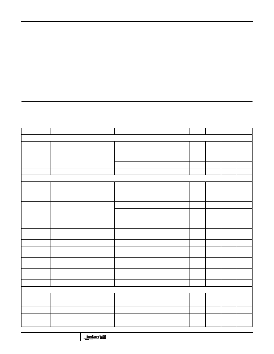
Electrical Specifications
V
DD
= 5V, V
BOOST
= 11V, I
LOAD
= 40mA, V
ON
= 15V, V
OFF
= -5V, V
LOGIC
= 2.5V, over temperature from -
40∞C to 85∞C, unless otherwise specified.
PARAMETER
DESCRIPTION
CONDITION
MIN
TYP
MAX
UNIT
SUPPLY
V
S
Supply Voltage
3
5.5
V
I
S
Quiescent Current
Enabled, LX not switching
1.6
2.5
mA
Disabled, EL7520
5
30
µA
Disabled, EL7520A
640
800
µA
F
OSC
Oscillator Frequency
900
1000
1100
kHz
BOOST
V
REF
Reference Voltage
T
A
= 25∞C
1.19
1.215
1.235
V
1.187
1.215
1.238
V
C
REF
V
REF
Capacitor
100
nF
V
FBB
Feedback Reference Voltage
T
A
= 25∞C
1.192
1.205
1.218
V
1.188
1.205
1.222
V
V
F_FBB
FBB Fault Trip Point
V
FBB
falling
1
V
D
MAX
Maximum Duty Cycle
85
%
Eff
Boost Efficiency
Test with 24m
R
DS(ON)
MOSFET,
I
LOAD
= 400mA
90
%
I(V
REF
)
Feedback Input Bias Current
PI mode, V
FBB
= 1.35V
50
500
nA
V
BOOST
/
V
IN
Line Regulation
C
INT
= 2.2nF, I
OUT
= 200mA
V
IN
= 3V to 5.5V
0.05
%/V
V
BOOST
/
I
BOOST
Load Regulation - "P" Mode
C
INT
pin strapped to V
DD
3
%
V
BOOST
/
I
BOOST
Load Regulation - "PI" Mode
I
OUT
= 10mA to 200mA
0.1
%
V
CINT_T
CINT Pl Mode Select Threshold
4.7
4.8
V
V
ON
LDO
V
FBP
FBP Regulation Voltage
I
DRVP
= 0.2mA, T
A
= 25∞C
1.181
1.211
1.229
V
I
DRVP
= 0.2mA
1.177
1.211
1.233
V
V
F_FBP
FBP Fault Trip Point
V
FBP
falling
0.95
1
1.05
V
I
FBP
FBP Input Bias Current
V
FBP
= 1.35V
-250
250
nA
GMP
FBP Effective Transconductance
V
DRVP
= 25V, I
DRVP
= 0.2 to 2mA
50
mS
EL7520, EL7520A

3
FN7318.0
July 12, 2005
V
ON
/
I(V
ON
)
V
ON
Load Regulation
I(V
ON
) = 0mA to 20mA
-0.5
%
I
DRVP
DRVP Sink Current
V
FBP
= 1.1V, V
DRVP
= 25V
2
4
mA
I
L_DRVP
DRVP Leakage Current
V
FBL
= 1.5V, V
DRVL
= 35V
0.1
5
µA
V
OFF
LDO
V
FBN
FBN Regulation Voltage
I
DRVN
= 0.2mA, T
A
= 25∞C
0.173
0.203
0.233
V
I
DRVN
= 0.2mA
0.171
0.203
0.235
V
V
F_FBN
FBN Fault Trip Point
V
FBN
falling
0.38
0.4
0.48
V
I
FBN
FBN Input Bias Current
V
FBN
= 1.25V
-250
250
nA
GMN
FBN Effective Transconductance
V
DRVN
= -6V, I
DRVN
= 0.2mA to 2mA
50
mS
V
OFF
/
I(V
OFF
)
V
OFF
Load Regulation
I(V
OFF
) = 0mA to 20mA
-0.15
%
I
DRVN
DRVN Source Current
V
FBN
= 0.3V, V
DRVN
= -6V
2
4
mA
I
L_DRVN
DRVN Leakage Current
V
FBN
= 0V, V
DRVN
= -20V
0.1
5
µA
V
LOGIC
LDO
V
FBL
FBL Regulation Voltage
I
DRVL
= 1mA, T
A
= 25∞C
1.176
1.2
1.224
V
I
DRVL
= 1mA
1.174
1.2
1.226
V
V
F_FBL
FBL Fault Trip Point
V
FBL
falling
0.90
1
1.05
V
I
FBL
FBL Input Bias Current
V
FBL
= 1.25V
-500
500
nA
GML
FBL Effective Transconductance
V
DRVL
= 2.5V, I
DRVP
= 1mA to 8mA
200
mS
V
LOGIC
/
I(V
LOGIC
)
V
LOGIC
Load Regulation
I(V
LOGIC
) = 0mA to 500mA
-0.5
%
I
DRVL
DRVL Sink Current
V
FBL
= 1.1V, V
DRVL
= 2.5V
5
16
mA
I
L
_
DRVL
DRVL Leakage Current
V
FBL
= 1.5V, V
DRVL
= 5.5V
0.1
5
µA
SEQUENCING
t
ON
Turn On Delay
C
DLY
= 0.1µF
30
ms
t
SS
Soft-start Time
C
DLY
= 0.1µF
2
ms
t
DEL1
Delay Between A
VDD
and V
OFF
C
DLY
= 0.1µF
10
ms
t
DEL2
Delay Between V
ON
and V
OFF
C
DLY
= 0.1µF
17
ms
t
DEL3
Delay Between V
OFF
and Delayed
V
BOOST
C
DLY
= 0.1µF
10
ms
I
DELB
DELB Pull-down Current
V
DELB
> 0.6V
50
µA
V
DELB
< 0.6V
1.4
mA
C
DEL
Delay Capacitor
100
nF
FAULT DETECTION
T
FAULT
Fault Time Out
C
DLY
= 0.1µF
50
ms
OT
Over-temperature Threshold
140
∞C
I
PG
PG Pull-down Current
VPG > 0.6V
15
µA
VPG < 0.6V
1.7
mA
LOGIC
V
HI
Logic High Threshold
2.2
V
V
LO
Logic Low Threshold
0.8
V
I
LOW
Logic Low bias Current
-1
0.1
1
µA
I
HIGH
Logic High bias Current
12
18
24
µA
Electrical Specifications
V
DD
= 5V, V
BOOST
= 11V, I
LOAD
= 40mA, V
ON
= 15V, V
OFF
= -5V, V
LOGIC
= 2.5V, over temperature from -
40∞C to 85∞C, unless otherwise specified. (Continued)
PARAMETER
DESCRIPTION
CONDITION
MIN
TYP
MAX
UNIT
EL7520, EL7520A
4
FN7318.0
July 12, 2005
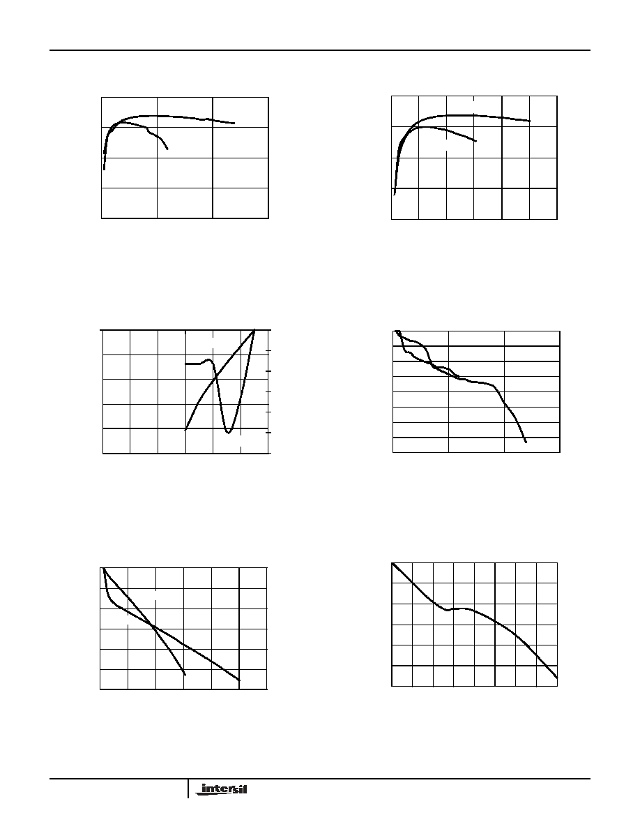
Typical Performance Curves
FIGURE 1. V
BOOST
EFFICIENCY vs I
OUT
(PI MODE)
FIGURE 2. V
BOOST
EFFICIENCY vs I
OUT
(P MODE)
FIGURE 3. V
BOOST
LINE REGULATION
FIGURE 4. V
BOOST
LOAD REGULATION (PI MODE)
FIGURE 5. V
BOOST
LOAD REGULATION (P MODE)
FIGURE 6. V
ON
LOAD REGULATION
60
70
80
90
100
0
500
1000
1500
I
OUT
(mA)
E
F
FICIE
NCY (%
)
V
IN
= 5V
V
IN
= 3V
60
70
80
90
100
0
200
400
600
800
1000
1200
I
OUT
(mA)
EFFICIENCY (%)
V
IN
= 5V
V
IN
= 3V
P MODE
PI MODE
-2.5
-2
-1.5
-1
-0.5
0
0
1
2
3
4
5
6
V
IN
(V)
LINE
REGUL
A
TION (
%
)
-0.03
-0.025
-0.02
-0.015
-0.01
-0.005
0
-0.4
-0.35
-0.3
-0.25
-0.2
-0.15
-0.1
-0.05
0
0
500
1000
1500
I
OUT
(mA)
LO
AD REG
U
LA
TIO
N
(%
)
V
IN
= 5V
V
IN
= 3V
-6
-5
-4
-3
-2
-1
0
0
200
400
600
800
1000
1200
I
OUT
(mA)
LOAD REGULA
T
I
ON (%)
V
IN
= 3V
V
IN
= 5V
L
O
AD REGUL
A
TION (
%
)
I
OUT
(mA)
0
-0.1
-0.3
-0.5
-0.6
0
20
40
60
80
-0.4
-0.2
EL7520, EL7520A
5
FN7318.0
July 12, 2005
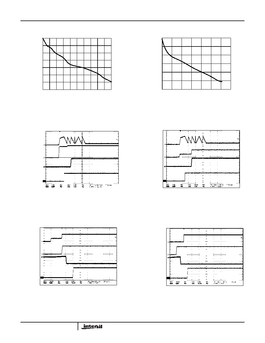
FIGURE 7. V
OFF
LOAD REGULATION
FIGURE 8. V
LOGIC
LOAD REGULATION
FIGURE 9. EL7520 START-UP SEQUENCE
FIGURE 10. EL7520 START-UP SEQUENCE
FIGURE 11. EL7520 START-UP SEQUENCE
FIGURE 12. EL7520 START-UP SEQUENCE
Typical Performance Curves
(Continued)
LO
AD REG
U
LA
TIO
N
(%
)
I
OUT
(mA)
0
-0.2
-0.8
-1.2
-1.4
0
20
60
80
100
-1
-0.6
40
-0.4
LO
AD REG
U
LA
TI
ON
(%)
I
OUT
(mA)
0
-0.2
-0.6
-1
-1.2
0
100
200
500
700
-0.8
-0.4
400
300
600
TIME (20ms/DIV)
V
CDLY
EN
V
LOGIC
V
REF
C
DLY
=0.1µF
V
CDLY
V
REF
V
LOGIC
V
BOOST
TIME (20ms/DIV)
C
DLY
=0.1µF
V
BOOST
V
LOGIC
V
OFF
V
ON
TIME (10ms/DIV)
C
DLY
=0.1µF
V
OFF
V
ON
V
LOGIC
TIME (20ms/DIV)
C
DLY
=0.1µF
V
BOOST-DELAY
EL7520, EL7520A