 | ÐлекÑÑоннÑй компоненÑ: EL7530 | СкаÑаÑÑ:  PDF PDF  ZIP ZIP |
Äîêóìåíòàöèÿ è îïèñàíèÿ www.docs.chipfind.ru
1
®
FN7434.3
EL7530
Monolithic 600mA Step-Down Regulator
with Low Quiescent Current
The EL7530 is a synchronous, integrated FET 600mA step-
down regulator with internal compensation. It operates with
an input voltage range from 2.5V to 5.5V, which
accommodates supplies of 3.3V, 5V, or a Li-Ion battery
source. The output can be externally set from 0.8V to V
IN
with a resistive divider.
The EL7530 features automatic PFM/PWM mode control, or
PWM mode only. The PWM frequency is typically 1.4MHz
and can be synchronized up to 12MHz. The typical no load
quiescent current is only 120µA. Additional features include
a Power-Good output, <1µA shut-down current, short-circuit
protection, and over-temperature protection.
The EL7530 is available in the 10-pin MSOP package,
making the the entire converter occupy less than 0.18n
2
of
PCB area with components on one side only. The 10-pin
MSOP package is specified for operation over the full -40°C
to +85°C temperature range.
Features
· Less than 0.18in
2
footprint for the complete 600mA
converter
· Components on one side of PCB
· Max height 1.1mm MSOP10
· Power-Good (PG) output
· Internally-compensated voltage mode controller
· Up to 95% efficiency
· <1µA shut-down current
· 120µA quiescent current
· Overcurrent and over-temperature protection
· External synchronizable up to 12MHz
· Pb-Free plus anneal available (RoHS compliant)
Applications
· PDA and pocket PC computers
· Bar code readers
· Cellular phones
· Portable test equipment
· Li-Ion battery powered devices
· Small form factor (SFP) modules
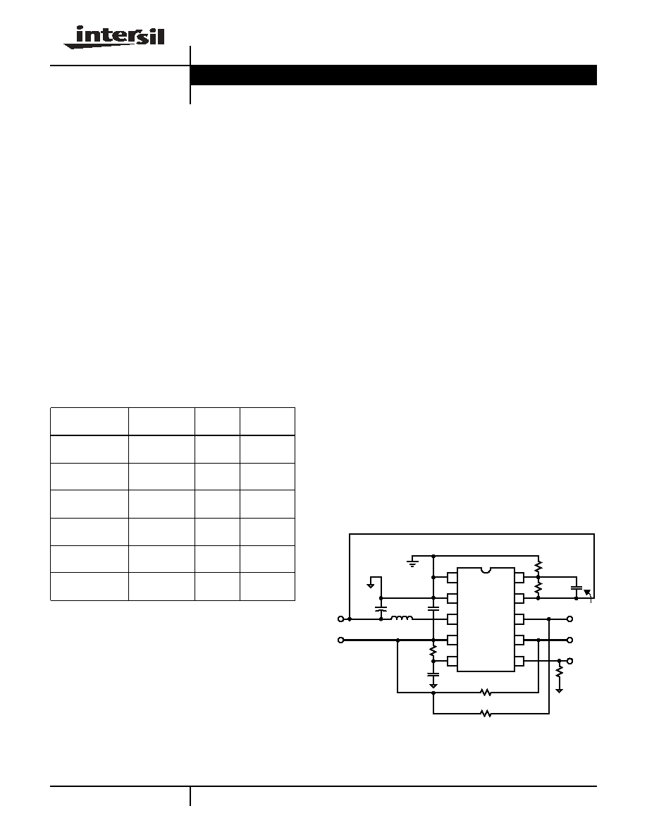
Pinout and Typical Application Diagram
EL7530
TOP VIEW
Ordering Information
PART NUMBER
(BRAND)
PACKAGE
TAPE &
REEL
PKG.
DWG. #
EL7530IY
(BYAAA)
10-Pin MSOP
-
MDP0043
EL7530IY-T7
(BYAAA)
10-Pin MSOP
7"
MDP0043
EL7530IY-T13
(BYAAA)
10-Pin MSOP
13"
MDP0043
EL7530IYZ
(BAADA) (Note)
10-Pin MSOP
(Pb-free)
-
MDP0043
EL7530IYZ-T7
(BAADA) (Note)
10-Pin MSOP
(Pb-free)
7"
MDP0043
EL7530IYZ-T13
(BAADA) (Note)
10-Pin MSOP
(Pb-free)
13"
MDP0043
NOTE: Intersil Pb-free plus anneal products employ special
Pb-free material sets; molding compounds/die attach materials
and 100% matte tin plate termination finish, which are RoHS
compliant and compatible with both SnPb and Pb-free soldering
operations. Intersil Pb-free products are MSL classified at Pb-free
peak reflow temperatures that meet or exceed the Pb-free
requirements of IPC/JEDEC J STD-020.
* V
O
= 0.8V * (1 + R
2
/ R
1
)
SGND
FB
VDD
SYNC
VIN
EN
LX
PG
PGND
VO
1.8µH
V
O
(1.8V@600mA)
C
1
PG
R
2
*
R
1
*
124k
100k
EN
SYNC
100k
C
2
V
S
(2.5V-6V)
100k
R
4
R
5
10µF
10µF
L
1
R
6
100k
0.1µF
R
3
100
C
3
C
4
470pF
1
2
3
4
10
9
8
7
5
6
Data Sheet
August 10, 2005
CAUTION: These devices are sensitive to electrostatic discharge; follow proper IC Handling Procedures.
1-888-INTERSIL or 1-888-468-3774
|
Intersil (and design) is a registered trademark of Intersil Americas Inc.
Copyright © Intersil Americas Inc. 2004-2005. All Rights Reserved.
All other trademarks mentioned are the property of their respective owners.
2
FN7434.3
August 10, 2005
IMPORTANT NOTE: All parameters having Min/Max specifications are guaranteed. Typ values are for information purposes only. Unless otherwise noted, all tests are
at the specified temperature and are pulsed tests, therefore: T
J
= T
C
= T
A
NOTE:
1.
JA
is measured in free air with the component mounted on a high effective thermal conductivity test board with "direct attach" features. See
Tech Brief TB379.
Absolute Maximum Ratings
(T
A
= 25°C)
Thermal Information
V
IN
, V
DD
, PG to SGND . . . . . . . . . . . . . . . . . . . . . . . -0.3V to +6.5V
LX to PGND . . . . . . . . . . . . . . . . . . . . . . . . . . -0.3V to (V
IN
+ +0.3V)
SYNC, EN, V
O
, FB to SGND . . . . . . . . . . . . . -0.3V to (V
IN
+ +0.3V)
PGND to SGND . . . . . . . . . . . . . . . . . . . . . . . . . . . . . -0.3V to +0.3V
Peak Output Current . . . . . . . . . . . . . . . . . . . . . . . . . . . . . . . 800mA
Thermal Resistance (Typical)
JA
(°C/W)
MSOP10 Package (Note 1) . . . . . . . . . . . . . . . . . . .
115
Operating Ambient Temperature . . . . . . . . . . . . . . . .-40°C to +85°C
Storage Temperature . . . . . . . . . . . . . . . . . . . . . . . .-65°C to +150°C
Junction Temperature . . . . . . . . . . . . . . . . . . . . . . . . . . . . . . +125°C
CAUTION: Stresses above those listed in "Absolute Maximum Ratings" may cause permanent damage to the device. This is a stress only rating and operation of the
device at these or any other conditions above those indicated in the operational sections of this specification is not implied.
Electrical Specifications
V
DD
= V
IN
= V
EN
= 3.3V, C1 = C2 = 10µF, L = 1.8µH, V
O
= 1.8V (as shown in Typical Application Diagram),
unless otherwise specified.
PARAMETER
DESCRIPTION
CONDITIONS
MIN
TYP
MAX
UNIT
DC CHARACTERISTICS
V
FB
Feedback Input Voltage
PWM Mode
790
800
810
mV
I
FB
Feedback Input Current
100
nA
V
IN
, V
DD
Input Voltage
2.5
5.5
V
V
IN,OFF
Minimum Voltage for Shutdown
V
IN
falling
2
2.2
V
V
IN,ON
Maximum Voltage for Startup
V
IN
rising
2.2
2.4
V
I
S
Input Supply Quiescent Current
Active - PFM Mode
V
SYNC
= 0V
120
145
µA
Active - PWM Mode
V
SYNC
= 3.3V
6.5
7.5
mA
I
DD
Supply Current
PWM, V
IN
= V
DD
= 5V
400
500
µA
EN = 0, V
IN
= V
DD
= 5V
0.1
1
µA
R
DS(ON)-PMOS
PMOS FET Resistance
V
DD
= 5V, wafer test only
70
100
m
R
DS(ON)-NMOS
NMOS FET Resistance
V
DD
= 5V, wafer test only
45
75
m
I
LMAX
Current Limit
1.2
A
T
OT,OFF
Over-temperature Threshold
T rising
145
°C
T
OT,ON
Over-temperature Hysteresis
T falling
130
°C
I
EN
, I
SYNC
EN, SYNC Current
V
EN
, V
RSI
= 0V and 3.3V
-1
1
µA
V
EN1
, V
SYNC1
EN, SYNC Rising Threshold
V
DD
= 3.3V
2.4
V
V
EN2
, V
SYNC2
EN, SYNC Falling Threshold
V
DD
= 3.3V
0.8
V
V
PG
Minimum V
FB
for PG, WRT Targeted
V
FB
Value
V
FB
rising
95
%
V
FB
falling
86
%
V
OLPG
PG Voltage Drop
I
SINK
= 3.3mA
35
70
mV
AC CHARACTERISTICS
F
PWM
PWM Switching Frequency
1.25
1.4
1.6
MHz
t
SYNC
Minimum SYNC Pulse Width
Guaranteed by design
25
ns
t
SS
Soft-start Time
650
µs
EL7530
3
FN7434.3
August 10, 2005
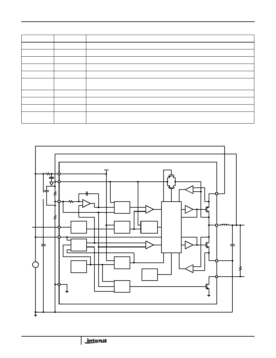
Block Diagram
Pin Descriptions
PIN NUMBER
PIN NAME
PIN FUNCTION
1
SGND
Negative supply for the controller stage
2
PGND
Negative supply for the power stage
3
LX
Inductor drive pin; high current digital output with average voltage equal to the regulator output voltage
4
VIN
Positive supply for the power stage
5
VDD
Power supply for the controller stage
6
SYNC
SYNC input pin; when connected to HI, regulator runs at forced PWM mode; when connected to Low, auto
PFM/PWM mode; when connected to external sync signal, at external PWM frequency up to 12MHz
7
EN
Enable
8
PG
Power-Good open drain output
9
VO
Output voltage sense
10
FB
Voltage feedback input; connected to an external resistor divider between V
O
and SGND for variable
output
-
+
-
+
-
+
-
+
-
+
CONTROL
LOGIC
PFM
ON-TIME
CONTROL
PWM
COMPEN-
SATION
RAMP
GENERA-
TOR
UNDER-
VOLTAGE
LOCKOUT
POWER
GOOD
CLOCK
SOFT-
START
BANDGAP
REFERENCE
TEMPERA-
TURE
SENSE
+
V
IN
LX
PGND
PG
V
O
FB
SYNC
EN
V
DD
SGND
10pF
5M
124K
100K
10µF
5V
SYNC
EN
PWM
COMPARATOR
PWM
COMPARATOR
SYNCHRONOUS
RECTIFIER
N-DRIVER
P-DRIVER
CURRENT
SENSE
INDUCTOR SHORT
1.8µH
10µF
100K
PG
1.8V
0 TO 600mA
100
0.1µF
C4
470pF
EL7530
4
FN7434.3
August 10, 2005
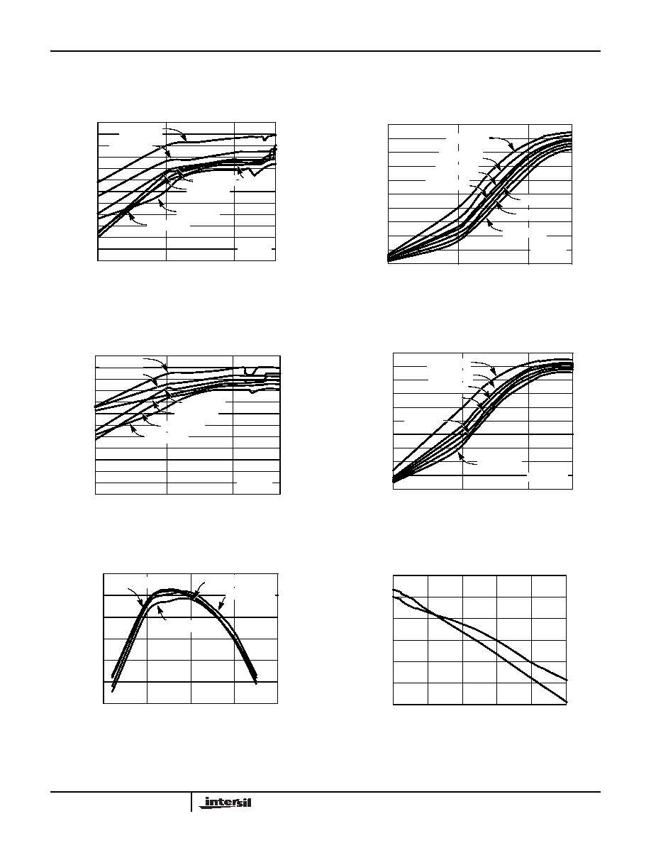
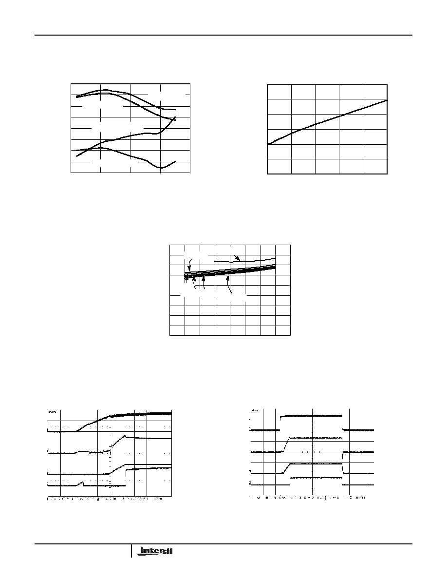
Performance Curves and Waveforms
All waveforms are taken at V
IN
=3.3V, V
O
=1.8V, I
O
=600mA with component values shown on page 1 at room ambient temperature, unless
otherwise noted.
FIGURE 1.
EFFICIENCY vs
I
O (PFM/PWM MODE)
FIGURE 2. EFFICIENCY vs I
O
(PWM MODE)
FIGURE 3. EFFICIENCY vs I
O
(PFM/FWM MODE)
FIGURE 4. EFFICIENCY vs I
O
(PWM MODE)
FIGURE 5. F
S
vs JUNCTION TEMPERATURE (PWM MODE)
FIGURE 6. LOAD REGULATIONS (PWM MODE)
40
45
50
55
60
65
70
75
80
85
90
95
100
1
10
100
600
I
O
(mA)
EFFICIENCY (%)
V
O
=3.3V
V
O
=2.5V
V
O
=1.8V
V
O
=1.5V
V
O
=1.2V
V
IN
=5V
V
O
=1.0V
V
O
=0.8V
0
10
20
30
40
50
60
70
80
90
100
1
10
100
600
I
O
(mA)
EFFICIENCY (%
)
V
O
=3.3V
V
O
=2.5V
V
O
=1.2V
V
O
=0.8V
V
IN
=5V
V
O
=1.0V
V
O
=1.8V
V
O
=1.5V
40
45
50
55
60
65
70
75
80
85
90
95
100
1
10
100
600
I
O
(mA)
EFFIC
I
ENCY (%)
V
O
=2.5V
V
O
=1.5V
V
O
=1.2V
V
O
=0.8V
V
IN
=3.3V
V
O
=1.0V
V
O
=1.8V
0
10
20
40
50
60
70
80
90
100
1
10
100
600
I
O
(mA)
EFFICI
ENC
Y
(
%
)
30
V
O
=2.5V
V
O
=1.8V
V
O
=1.5V
V
O
=1.2V
V
O
=1.0V
V
O
=0.8V
V
IN
=3.3V
1.32
1.34
1.36
1.38
1.4
1.42
1.44
-50
0
50
100
150
T
A
(°C)
F
S
(M
H
z
)
V
IN
=5V I
O
=600mA
V
IN
=3.3V I
O
=600mA
V
IN
=5V I
O
=0A
V
IN
=3.3V I
O
=0A
-0.5%
-0.4%
-0.3%
-0.2%
-0.1%
0.0%
0.1%
0
0.2
0.4
0.6
0.8
1
I
O
(A)
V
O
CHANGES
V
IN
=3.3V
V
IN
=5V
EL7530
5
FN7434.3
August 10, 2005
FIGURE 7. PWM MODE LOAD/LINE REGULATIONS vs
JUNCTION TEMPERATURE
FIGURE 8. NO LOAD QUIESCENT CURRENT (PWM MODE)
FIGURE 9. NO LOAD QUIESCENT CURRENT (PFM MODE)
FIGURE 10. START-UP AT I
O
= 600mA
FIGURE 11. ENABLE AND SHUT-DOWN
Performance Curves and Waveforms
(Continued)
All waveforms are taken at V
IN
=3.3V, V
O
=1.8V, I
O
=600mA with component values shown on page 1 at room ambient temperature, unless
otherwise noted.
-0.7%
-0.6%
-0.5%
-0.4%
-0.3%
-0.2%
-0.1%
0.0%
0.1%
-50
0
50
100
150
T
J
(°C)
V
O
CHANGE
S
V
IN
=5V I
O
=600mA
V
IN
=3.3V I
O
=600mA
V
IN
=3.3V I
O
=0A
V
IN
=5V I
O
=0A
0
2
4
6
8
10
12
2.5
3
3.5
4
4.5
5
V
S
(V)
I
S
(m
A
)
140
130
120
100
90
80
70
60
50
2.0
2.5
3.5
4.5
5.0
6.0
V
S
(V)
I
S
(µ
A
)
V
O
=3.3V
V
O
=1.8V
V
O
=1.5V
V
O
=1.2V V
O
=1.0V
V
O
=0.8V
110
3.0
4.0
5.5
V
IN
(2V/DIV)
I
IN
(0.25A/DIV)
V
O
(2V/DIV)
200µs/DIV
PG
EN
V
O
(2V/DIV)
I
IN
(0.25A/DIV)
500µs/DIV
PG
2
EL7530
1