Äîêóìåíòàöèÿ è îïèñàíèÿ www.docs.chipfind.ru
1
®
FN7396.5
EL7536
Monolithic 1A Step-Down Regulator
The EL7536 is a synchronous, integrated FET 1A step-down
regulator with internal compensation. It operates with an
input voltage range from 2.5V to 5.5V, which accommodates
supplies of 3.3V, 5V, or a Li-Ion battery source. The output
can be externally set from 0.8V to V
IN
with a resistive
divider.
The EL7536 features PWM mode control. The operating
frequency is typically 1.4MHz. Additional features include a
100ms Power-On-Reset output, <1µA shut-down current,
short-circuit protection, and over-temperature protection.
The EL7536 is available in the 10-pin MSOP package,
making the entire converter occupy less than 0.15in
2
of PCB
area with components on one side only. Both packages are
specified for operation over the full -40°C to +85°C
temperature range.
Features
· Less than 0.15in
2
(0.97cm
2
) footprint for the complete 1A
converter
· Components on one side of PCB
· Max height 1.1mm MSOP10
· 100ms Power-On-Reset output (POR)
· Internally-compensated voltage mode controller
· Up to 94% efficiency
· <1µA shut-down current
· Overcurrent and over-temperature protection
· Pb-Free plus anneal available (RoHS compliant)
Applications
· PDA and pocket PC computers
· Bar code readers
· Cellular phones
· Portable test equipment
· Li-Ion battery powered devices
· Small form factor (SFP) modules
Pinout and Typical Application Diagram
EL7536
TOP VIEW
Ordering Information
PART NUMBER
(BRAND)
PACKAGE
TAPE &
REEL
PKG.
DWG. #
EL7536IY
(BDAAA)
10-Pin MSOP
-
MDP0043
EL7536IY-T7
(BDAAA)
10-Pin MSOP
7"
MDP0043
EL7536IY-T13
(BDAAA)
10-Pin MSOP
13"
MDP0043
EL7536IYZ
(BFAAA) (Note)
10-Pin MSOP
(Pb-free)
-
MDP0043
EL7536IYZ-T7
(BFAAA) (Note)
10-Pin MSOP
(Pb-free)
7"
MDP0043
EL7536IYZ-T13
(BFAAA) (Note)
10-Pin MSOP
(Pb-free)
13"
MDP0043
NOTE: Intersil Pb-free plus anneal products employ special Pb-free
material sets; molding compounds/die attach materials and 100%
matte tin plate termination finish, which are RoHS compliant and
compatible with both SnPb and Pb-free soldering operations. Intersil
Pb-free products are MSL classified at Pb-free peak reflow
temperatures that meet or exceed the Pb-free requirements of
IPC/JEDEC J STD-020.
* V
O
= 0.8V * (1 + R
2
/ R
1
)
1
2
3
4
10
9
8
7
5
6
SGND
FB
VDD
RSI
VIN
EN
LX
POR
PGND
VO
1.8µH
V
O
(1.8V@1A)
C
1
POR
R
2
*
R
1
*
124k
100k
EN
RSI
100k
C
2
V
IN
(2.5V-6V)
100k
R
4
R
5
10µF
10µF
L
1
R
6
100k
0.1µF
R
3
100
C
3
Data Sheet
CAUTION: These devices are sensitive to electrostatic discharge; follow proper IC Handling Procedures.
1-888-INTERSIL or 1-888-468-3774
|
Intersil (and design) is a registered trademark of Intersil Americas Inc.
Copyright © Intersil Americas Inc. 2003-2005. All Rights Reserved.
All other trademarks mentioned are the property of their respective owner
s.
August 10, 2005
2
FN7396.5
August 10, 2005
IMPORTANT NOTE: All parameters having Min/Max specifications are guaranteed. Typ values are for information purposes only. Unless otherwise noted, all tests are
at the specified temperature and are pulsed tests, therefore: T
J
= T
C
= T
A
Absolute Maximum Ratings
(T
A
= 25°C)
V
IN
, V
DD
, POR to SGND . . . . . . . . . . . . . . . . . . . . . . -0.3V to +6.5V
LX to PGND . . . . . . . . . . . . . . . . . . . . . . . . . . -0.3V to (V
IN
+ +0.3V)
RSI, EN, V
O
, FB to SGND . . . . . . . . . . . . . . . -0.3V to (V
IN
+ +0.3V)
PGND to SGND . . . . . . . . . . . . . . . . . . . . . . . . . . . . . -0.3V to +0.3V
Peak Output Current . . . . . . . . . . . . . . . . . . . . . . . . . . . . . . . . . 1.2A
Operating Ambient Temperature . . . . . . . . . . . . . . . .-40°C to +85°C
Storage Temperature . . . . . . . . . . . . . . . . . . . . . . . .-65°C to +150°C
Junction Temperature . . . . . . . . . . . . . . . . . . . . . . . . . . . . . . +145°C
CAUTION: Stresses above those listed in "Absolute Maximum Ratings" may cause permanent damage to the device. This is a stress only rating and operation of the
device at these or any other conditions above those indicated in the operational sections of this specification is not implied.
Electrical Specifications
V
DD
= V
IN
= V
EN
= 3.3V, C1 = C2 = 10µF, L = 1.8µH, V
O
= 1.8V, unless otherwise specified.
PARAMETER
DESCRIPTION
CONDITIONS
MIN
TYP
MAX
UNIT
DC CHARACTERISTICS
V
FB
Feedback Input Voltage
790
800
810
mV
I
FB
Feedback Input Current
250
nA
V
IN
, V
DD
Input Voltage
2.5
5.5
V
V
IN,OFF
Minimum Voltage for Shutdown
V
IN
falling
2
2.2
V
V
IN,ON
Maximum Voltage for Startup
V
IN
rising
2.2
2.4
V
I
DD
Supply Current
PWM, V
IN
= V
DD
= 5V
400
500
µA
EN = 0, V
IN
= V
DD
= 5V
0.1
1
µA
R
DS(ON)-PMOS
PMOS FET Resistance
V
DD
= 5V, wafer test only
70
100
m
R
DS(ON)-NMOS
NMOS FET Resistance
V
DD
= 5V, wafer test only
45
75
m
I
LMAX
Current Limit
1.5
A
T
OT,OFF
Over-temperature Threshold
T rising
145
°C
T
OT,ON
Over-temperature Hysteresis
T falling
130
°C
I
EN
, I
RSI
EN, RSI Current
V
EN
, V
RSI
= 0V and 3.3V
-1
1
V
V
EN1
, V
RSI1
EN, RSI Rising Threshold
V
DD
= 3.3V
2.4
V
V
EN2
, V
RSI2
EN, RSI Falling Threshold
V
DD
= 3.3V
0.8
V
V
POR
Minimum V
FB
for POR, WRT Targeted
V
FB
Value
V
FB
rising
95
%
V
FB
falling
86
%
V
OLPOR
POR Voltage Drop
I
SINK
= 5mA
35
70
mV
AC CHARACTERISTICS
F
PWM
PWM Switching Frequency
1.4
1.5
1.75
MHz
t
RSI
Minimum RSI Pulse Width
Guaranteed by design
25
50
ns
t
SS
Soft-start Time
650
µs
t
POR
Power On Reset Delay Time
80
100
120
ms
EL7536
3
FN7396.5
August 10, 2005
Block Diagram
Pin Descriptions
PIN NUMBER
PIN NAME
PIN FUNCTION
1
SGND
Negative supply for the controller stage
2
PGND
Negative supply for the power stage
3
LX
Inductor drive pin; high current digital output with average voltage equal to the regulator output voltage
4
VIN
Positive supply for the power stage
5
VDD
Power supply for the controller stage
6
RSI
Resets POR timer
7
EN
Enable
8
POR
Power on reset open drain output
9
VO
Output voltage sense
10
FB
Voltage feedback input; connected to an external resistor divider between V
O
and SGND for variable
output
-
+
-
+
-
+
CONTROL
LOGIC
PWM
COMPEN-
SATION
UNDER-
VOLTAGE
LOCKOUT
POR
CLOCK
1.4MHz
SOFT-
START
BANDGAP
REFERENCE
TEMPERATURE
SENSE
+
V
IN
LX
PGND
POR
V
O
FB
EN
V
DD
SGND
10pF
5M
124K
100K
10µF
2.5V-
3.5V
EN
PWM
COMPARATOR
N-DRIVER
P-DRIVER
CURRENT
LIMIT
1.8µ
10µF
100K
PG
1.8V
1A
RSI
RAMP
GENERATOR
EL7536
4
FN7396.5
August 10, 2005
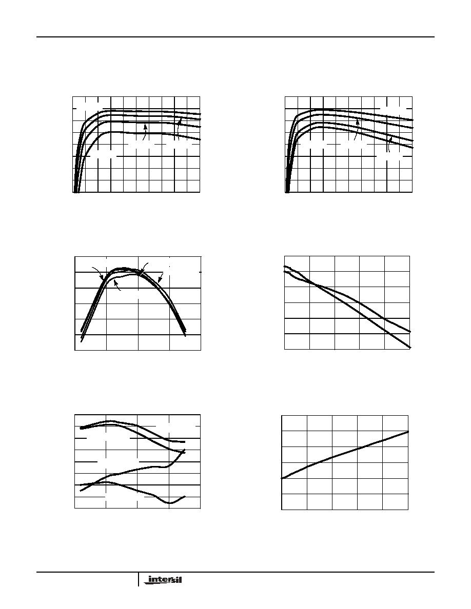
Performance Curves and Waveforms
All waveforms are taken at V
IN
=3.3V, V
O
=1.8V, I
O
=1A with component values shown on page 1 at room ambient temperature, unless otherwise
noted.
FIGURE 1. EFFICIENCY
FIGURE 2. EFFICIENCY
FIGURE 3. F
S
vs JUNCTION TEMPERATURE
FIGURE 4. LOAD REGULATIONS
FIGURE 5. LOAD/LINE REGULATIONS vs JUNCTION
TEMPERATURE
FIGURE 6. NO LOAD INPUT CURRENT
V
IN
=5V
100
95
90
85
80
75
70
65
60
0
200
400
600
800
1000
I
O
(mA)
EFFIC
I
ENCY (%)
V
O
=3.3V
V
O
=1.2V
V
O
=2.5V
V
O
=1.8V
V
IN
=3.3V
100
95
90
85
80
75
70
65
60
0
200
400
600
800
1000
I
O
(mA)
EFFIC
I
ENCY (%)
V
O
=2.5V
V
O
=1V
V
O
=1.2V
V
O
=1.8V
1.32
1.34
1.36
1.38
1.4
1.42
1.44
-50
0
50
100
150
T
A
(°C)
F
S
(MHz
)
V
IN
=5V I
O
=1A
V
IN
=3.3V I
O
=1A
V
IN
=5V I
O
=0A
V
IN
=3.3V I
O
=0A
-0.5%
-0.4%
-0.3%
-0.2%
-0.1%
0.0%
0.1%
0
0.2
0.4
0.6
0.8
1
I
O
(A)
V
O
CHANGES
V
IN
=3.3V
V
IN
=5V
-0.7%
-0.6%
-0.5%
-0.4%
-0.3%
-0.2%
-0.1%
0.0%
0.1%
-50
0
50
100
150
T
J
(°C)
V
O
C
HANGES
V
IN
=5V I
O
=1A
V
IN
=3.3V I
O
=1A
V
IN
=3.3V I
O
=0A
V
IN
=5V I
O
=0A
0
2
4
6
8
10
12
2.5
3
3.5
4
4.5
5
V
IN
(V)
I
IN
(mA)
EL7536
5
FN7396.5
August 10, 2005
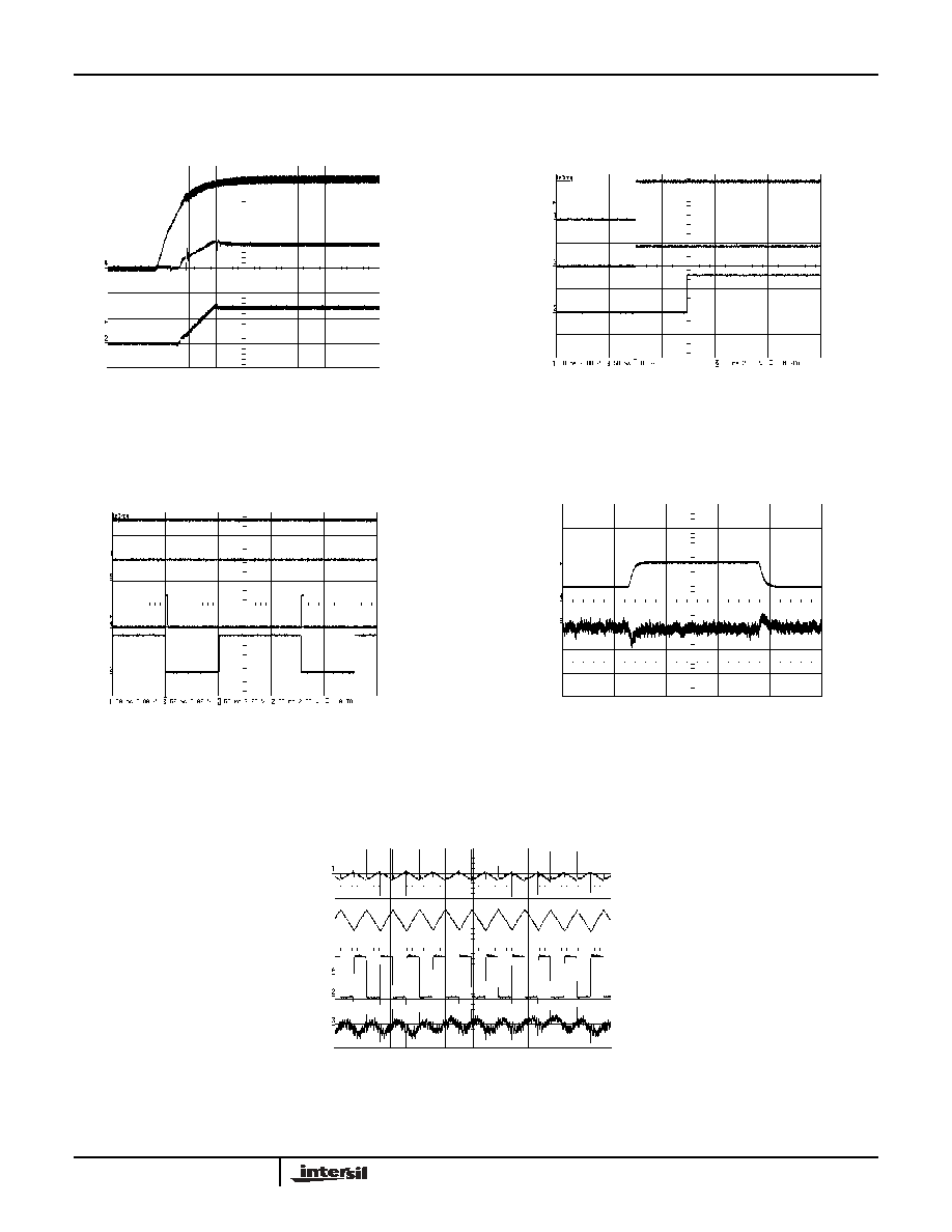
FIGURE 7. START-UP 1
FIGURE 8. START-UP 2
FIGURE 9. POR FUNCTION
FIGURE 10. TRANSIENT RESPONSE
FIGURE 11. STEADY-STATE
Performance Curves and Waveforms
(Continued)
All waveforms are taken at V
IN
=3.3V, V
O
=1.8V, I
O
=1A with component values shown on page 1 at room ambient temperature, unless otherwise
noted.
V
IN
(1V/d)
I
IN
(0.5A/d)
V
O
(1V/d)
0.5ms/d
V
IN
(2V/d)
POR
(2V/d)
V
O
(2V/d)
50ms/d
V
IN
(2V/d)
POR
(2V/d)
V
O
(2V/d)
50ms/d
RSI
(2V/d)
0.75A
20mV/d
0.25A
0.2ms/d
I
O
V
O
100mV/d
10mV/d
0.5A/d
1µs/d
i
L
V
IN
V
O
V
LX
2V/d
EL7536