 | –≠–ª–µ–∫—Ç—Ä–æ–Ω–Ω—ã–π –∫–æ–º–ø–æ–Ω–µ–Ω—Ç: EL7554 | –°–∫–∞—á–∞—Ç—å:  PDF PDF  ZIP ZIP |
1
Æ
FN7360.2
EL7554
Monolithic 4 Amp DC-DC Step-Down
Regulator
The EL7554 is a full-feature synchronous 4A step-down
regulator capable of up to 96% efficiency. This device
operates from 3V to 6V V
IN
input supply. With internal
CMOS power FETs, the device can operate at up to 100%
duty ratio, allowing for output voltage range from 0.8V up to
nearly V
IN
.The adjustable high switching frequency of up to
1MHz enables the use of small components, making the
whole converter occupy less than 0.58 square inch with
components on one side of the PCB. The EL7554 operates
at constant frequency PWM mode, making external
synchronization possible. The EL7554 features soft-start
and full start-up control, which eliminates the in-rush current
and enables users to control the start-up of multiple
converters to any configuration with ease. The EL7554 also
offers a ±5% voltage margining capability that allows raising
and lowering of the supplies derived from the EL7554 to
validate the performance and reliability of system cards
quickly and easily during manufacturing testing. A junction
temperature indicator conveniently monitors the silicon die
temperature, saving designers time in the tedious thermal
characterization.
An easy-to-use simulation tool is available for
download
and
can be used to modify design parameters such as switching
frequency, voltage ripple, ambient temperature, as well as
view schematics waveforms, efficiency graphs, and
complete BOM with Gerber layout.
The EL7554 is available in a 28-pin HTSSOP package and
is specified for operation over the -40∞C to +85∞C
temperature range.
Features
∑ Integrated MOSFETs
∑ 4A continuous output current
∑ Up to 96% efficiency
∑ All ceramic capacitors
∑ Multiple supply start-up tracking
∑ Built-in ±5% voltage margining
∑ 3V to 6V input voltage
∑ 0.58 in
2
footprint with components on one side of PCB
∑ Adjustable switching frequency to 1MHz
∑ Oscillator synchronization possible
∑ 100% duty ratio
∑ Junction temperature indicator
∑ Over-temperature protection
∑ Internal soft-start
∑ Variable output voltage down to 0.8V
∑ Power-good indicator
∑ 28-pin HTSSOP package
∑ Pb-free available (RoHS compliant)
Applications
∑ Point-of-regulation power supplies
∑ FPGA Core and I/O supplies
∑ DSP, CPU Core, and IO supplies
∑ Logic/Bus supplies
∑ Portable equipment
Related Documentation
∑ Technical Brief 418 - Using the EL7554 Demo Board
∑ Easy to use applications software simulation tool available
at
www.intersil.com/dc-dc
Ordering Information
PART
NUMBER
PACKAGE
TAPE &
REEL
PKG. DWG. #
EL7554IRE
28-Pin HTSSOP
-
MDP0048
EL7554IRE-T7
28-Pin HTSSOP
7"
MDP0048
EL7554IRE-T13
28-Pin HTSSOP
13"
MDP0048
EL7554IREZ
(See Note)
28-Pin HTSSOP
(Pb-free)
-
MDP0048
EL7554IREZ-T7
(See Note)
28-Pin HTSSOP
(Pb-free)
7"
MDP0048
EL7554IREZ-
T13 (See Note)
28-Pin HTSSOP
(Pb-free)
13"
MDP0048
NOTE: Intersil Pb-free products employ special Pb-free material sets; molding
compounds/die attach materials and 100% matte tin plate termination finish, which are
RoHS compliant and compatible with both SnPb and Pb-free soldering operations.
Intersil Pb-free products are MSL classified at Pb-free peak reflow temperatures that
meet or exceed the Pb-free requirements of IPC/JEDEC J STD-020.
Data Sheet
January 31, 2005
CAUTION: These devices are sensitive to electrostatic discharge; follow proper IC Handling Procedures.
1-888-INTERSIL or 1-888-352-6832
|
Intersil (and design) is a registered trademark of Intersil Americas Inc.
Copyright Intersil Americas Inc. 2004, 2005. All Rights Reserved
All other trademarks mentioned are the property of their respective owners.

2
FN7360.2
January 31, 2005
Typical Application Diagram
0.018µF
0.018µF
2.2µH
47µF
V
OUT
(1.8V, 4A)
2x10µF
V
IN
(3V TO
6V)
0.22µF
220pF
COMP
VREF
FB
VO
VTJ
TM
SEL
LX
LX
LX
LX
LX
LX
NC
SGND
COSC
STN
STP
EN
PG
VDD
VIN
VIN
VIN
PGND
PGND
PGND
NC
1
2
3
4
28
27
26
25
5
6
7
24
23
22
8
21
9
10
20
19
11
12
13
18
17
16
14
15
R
2
R
1
2.32K
10.2K
12.7K
C
C
R
C
C
OUT
C
OSC
C
IN
EL7554
3
FN7360.2
January 31, 2005
IMPORTANT NOTE: All parameters having Min/Max specifications are guaranteed. Typ values are for information purposes only. Unless otherwise noted, all tests are
at the specified temperature and are pulsed tests, therefore: T
J
= T
C
= T
A
Absolute Maximum Ratings
(T
A
= 25∞C)
V
IN
, V
DD
to SGND. . . . . . . . . . . . . . . . . . . . . . . . . . . -0.3V to +6.5V
VX to PGND. . . . . . . . . . . . . . . . . . . . . . . . . . . . . -0.3V to V
IN
+0.3V
SGND to PGND . . . . . . . . . . . . . . . . . . . . . . . . . . . . . -0.3V to +0.3V
COMP, V
REF
, FB, V
O
, V
TJ
, TM,
SEL, PG, EN, STP, STN, C
OSC
to SGND . . . . . -0.3V to V
DD
+0.3V
Storage Temperature . . . . . . . . . . . . . . . . . . . . . . . .-65∞C to +150∞C
Junction Temperature . . . . . . . . . . . . . . . . . . . . . . . . . . . . . . +135∞C
Ambient Operating Temperature . . . . . . . . . . . . . . . .-40∞C to +85∞C
CAUTION: Stresses above those listed in "Absolute Maximum Ratings" may cause permanent damage to the device. This is a stress only rating and operation of the
device at these or any other conditions above those indicated in the operational sections of this specification is not implied.
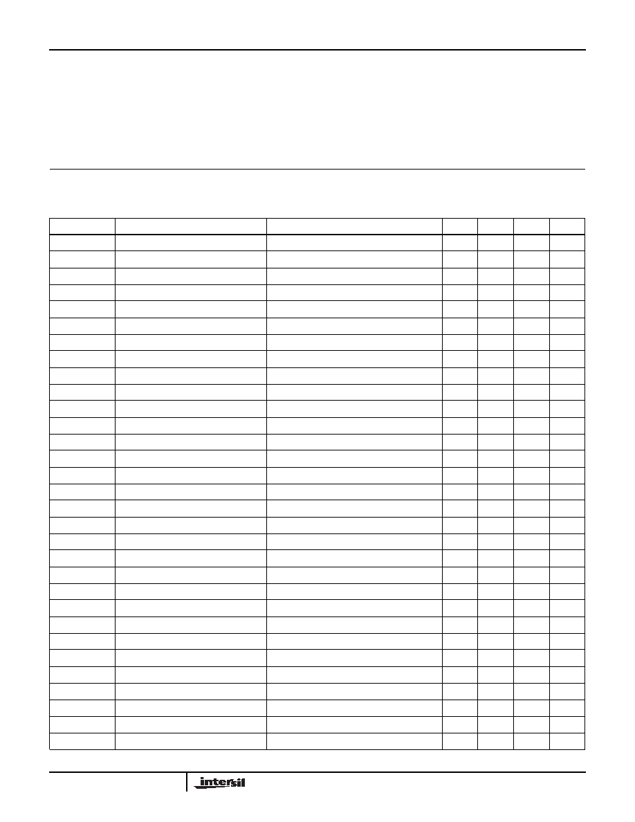
DC Electrical Specifications
V
DD
= V
IN
= 3.3V, T
A
= T
J
= 25∞C, C
OSC
= 390pF, Unless Otherwise Specified
PARAMETER
DESCRIPTION
CONDITIONS
MIN
TYP
MAX
UNIT
V
IN
Input Voltage Range
3
6
V
V
REF
Reference Accuracy
1.24
1.26
1.28
V
V
REFTC
Reference Temperature Coefficient
50
ppm/∞C
V
REFLOAD
Reference Load Regulation
0 < I
REF
< 50µA
-1
%
V
RAMP
Oscillator Ramp Amplitude
1.15
V
I
OSC_CHG
Oscillator Charge Current
0.1V < V
OSC
< 1.25V
200
µA
I
OSC_DIS
Oscillator Discharge Current
0.1V < V
OSC
< 1.25V
8
mA
I
VDD
V
DD
Supply Current
V
EN
= 1 (L disconnected)
2
2.7
5
mA
I
VDD_OFF
V
DD
Standby Current
EN = 0
1
1.5
mA
V
DD_OFF
V
DD
for Shutdown
2.4
2.65
V
V
DD_ON
V
DD
for Startup
2.6
2.95
V
T
OT
Over-temperature Threshold
135
∞C
T
HYS
Over-temperature Hysteresis
20
∞C
I
LEAK
Internal FET Leakage Current
EN = 0, L
X
= 6V (low FET), L
X
= 0V (high FET)
10
µA
I
LMAX
Peak Current Limit
6
A
R
DSON1
PFET On Resistance
35
70
m
R
DSONTC2
NFET On Resistance
30
60
m
R
DSONTC
R
DSON
Tempco
0.2
m
/∞C
I
STP
STP Pin Input Pull-down Current
V
STP
= V
IN
/2
-4
2.5
µA
I
STN
STN Pin Input Pull-up Current
V
STN
= V
IN
/2
2.5
4
µA
V
PGP
Positive Power Good Threshold
With respect to target output voltage
6
14
%
V
PGN
Negative Power Good Threshold
With respect to target output voltage
-14
-6
%
V
PG_HI
Power Good Drive High
I
PG
= 1mA
2.6
V
V
PG_LO
Power Good Drive Low
I
PG
= -1mA
0.5
V
V
OVP
Output Over-voltage Protection
10
%
V
FB
Output Initial Accuracy
I
LOAD
= 0A
0.79
0.8
0.81
V
V
FB_LINE
Output Line Regulation
V
IN
= 3.3V,
V
IN
= 10%, I
LOAD
= 0A
0.2
0.5
%
GM
EA
Error Amplifier Transconductance
V
CC
= 0.65V
85
125
165
µs
V
FB_TC
Output Temperature Stability
0∞C < T
A
< 85∞C, I
LOAD
= 3A
±1
%
F
S
Switching Frequency
300
370
440
kHz
I
FB
Feedback Input Pull-up Current
V
FB
= 0V
100
200
nA
EL7554
4
FN7360.2
January 31, 2005
V
EN_HI
EN Input High Level
2.6
V
V
EN_LO
EN Input Low Level
1
V
I
EN
Enable Pull-up Current
V
EN
= 0
-4
-2.5
µA
TM, S
EL_HI
Input High Level
2.6
V
TM, S
EL_LO
Input Low Level
1
V
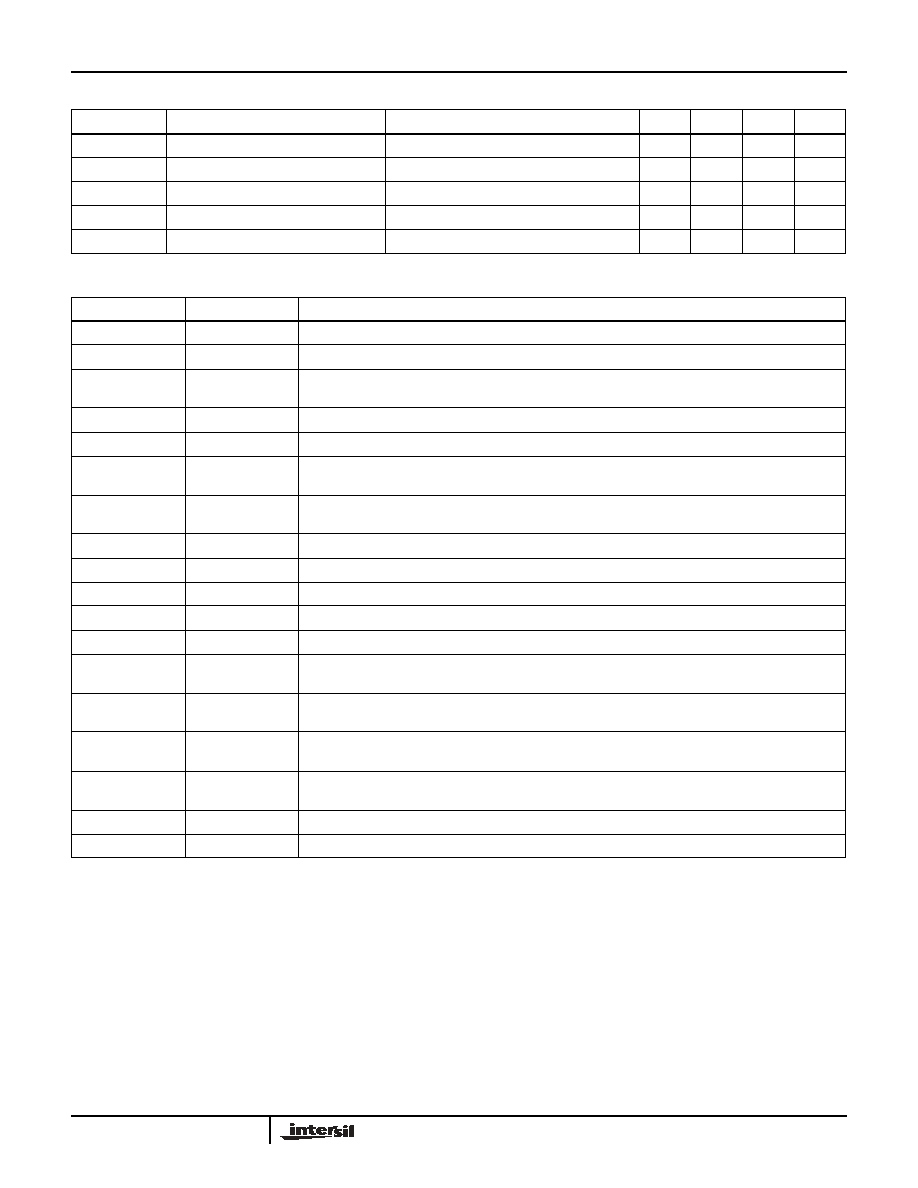
DC Electrical Specifications
V
DD
= V
IN
= 3.3V, T
A
= T
J
= 25∞C, C
OSC
= 390pF, Unless Otherwise Specified
PARAMETER
DESCRIPTION
CONDITIONS
MIN
TYP
MAX
UNIT
Pin Descriptions
PIN NUMBER
PIN NAME
PIN FUNCTION
1
COMP
Error amplifier output; place loop compensation components here
2
VREF
Bandgap reference bypass capacitor; typically 0.01µF to 0.047µF to SGND
3
FB
Voltage feedback input; connected to external resistor divider between V
OUT
and SGND for adjustable
output; also used for speed-up capacitor connection
4
VO
Output sense for fixed output; also used for speed-up capacitor connection
5
VTJ
Junction temperature monitor output, connected to a 0.01µF - 0.047µF to SGND
6
TM
Stress test enable; allows ±5% output movement; needs a pull-down resistor (1K - 100K); connect to
SGND if function is not used
7
SEL
Positive or negative voltage margining set pin; needs a pull-down resistor (1K - 100K); connect to
SGND if function is not used
8, 9, 10, 11, 12, 13
LX
Inductor drive pin; high current output whose average voltage equals the regulator output voltage
14, 15
NC
Not used
16, 17, 18
PGND
Ground return of the regulator; connected to the source of the low-side synchronous NMOS Power FET
19, 20, 21
VIN
Power supply input of the regulator; connected to the drain of the high-side PMOS Power FET
22
VDD
Control circuit positive supply; connected to V
IN
through an internal 20
resistor
23
PG
Power-good window comparator output; logic 1 when regulator output is within ±10% of target output
voltage
24
EN
Chip enable, active high; a 2µA internal pull-up current enables the device if the pin is left open; a
capacitor can be added at this pin to delay the start of a converter
25
STP
Auxilliary supply tracking positive input; tied to regulator output to synchronize start-up with a second
supply; leave open for standalone operation; 2µA internal pull-up current
26
STN
Auxiliary supply tracking negative input; connect to output of a second supply to synchronize start-up;
leave open for standalone operation; 2µA internal pull-up current
27
COSC
Oscillator timing capacitor (see performance curves)
28
SGND
Control circuit negative supply or signal ground
EL7554
5
FN7360.2
January 31, 2005
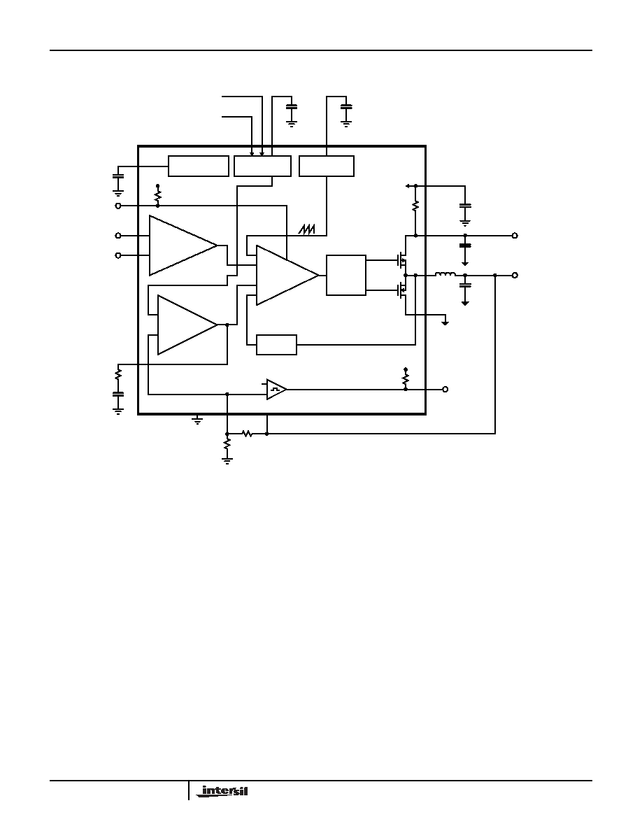
Block Diagram
DRIVERS
PWM
CONTROLLER
POWER
TRACKING
CURRENT
SENSE
VOLTAGE
REFERENCE
OSCILLATOR
2.2nF
STP
STN
SGND
POWER
POWER
FET
FET
220pF
0.018µF
2.2µH
V
OUT
(UP TO 4A)
47µF
V
REF
C
OSC
PGND
V
TJ
FB
EN
-
+
PG
V
REF
V
IN
V
IN
V
DD
2x10µF
V
O
R
2
V
DD
TM
SEL
20
EA
COMP
0.22µF
V
DD
R
1
R
C
C
C
JUNCTION
TEMPERATURE
EL7554