1
Æ
FN7339.1
EL7556D
Integrated Adjustable 6 Amp
Synchronous Switcher
The EL7556D is an adjustable synchronous DC:DC
switching regulator optimized for a 5V input and 1.0V-3.8V
output. By combining integrated NMOS power FETS with a
fused-lead package, the EL7556D can supply up to 6A
continuous output current without the use of external power
devices or discrete heat sinks, thereby minimizing design
effort and overall system cost.
On-chip resistorless current sensing is used to achieve
stable, highly efficient, current-mode control. The EL7556D
also incorporates the VCC2DET function to directly interface
with the Intel P54 and P55 microprocessors. Depending on
the state of VCC2DET, the output voltage is internally preset
to 3.5V or a user-adjustable voltage using two external
resistors. In both internal and external feedback modes the
active-high PWRGD output indicates when the regulator
output is within ±10% of the programmed voltage. An on-
board sensor monitors die temperature (OT) for over-
temperature conditions and can be connected directly to
OUTEN to provide automatic thermal shutdown. Adjustable
oscillator frequency and slope compensation allow added
flexibility in overall system design.
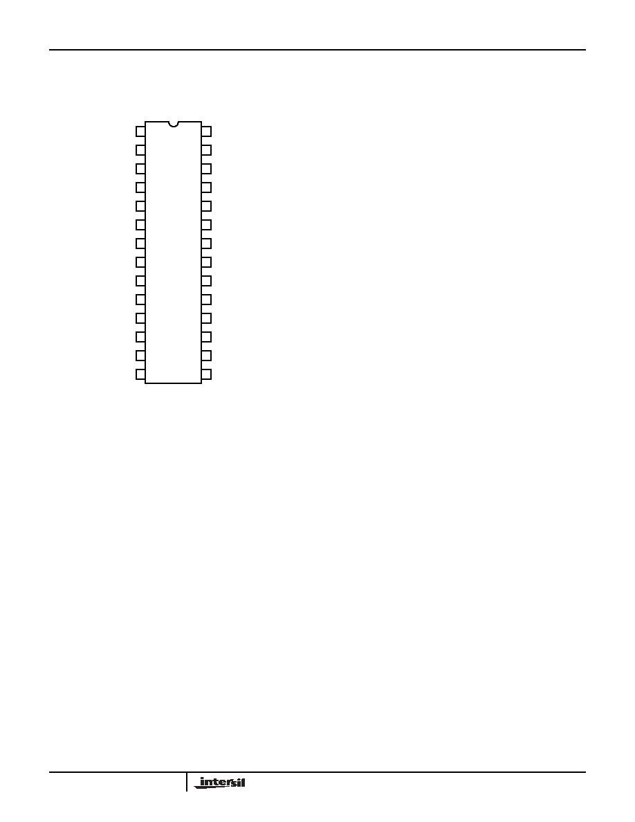
The EL7556D is available in a 28-pin SO package and is
specified for operation over the full -40∞C to +85∞C
temperature range.
Features
∑ Improved temperature and voltage ranges
∑ 6A continuous load current
∑ Precision internal 1% reference
∑ 1.0V to 3.8V output voltage
∑ Internal power MOSFETs
∑ >90% efficiency
∑ Synchronous switching
∑ Adjustable slope compensation
∑ Over-temperature indicator
∑ Pulse-by-pulse current limiting
∑ Operates up to 1MHz
∑ 1.5% typical output accuracy
∑ Adjustable oscillator with sync
∑ Remote enable/disable
∑ Intel P54- and P55-compatible
∑ VCC2DET interface
∑ Internal soft-start
∑ Pb-free plus anneal available (RoHS compliant)
Applications
∑ PC motherboards
∑ Local high power CPU supplies
∑ 5V to 1.0V DC:DC conversion
∑ Portable electronics/instruments
∑ P54 and P55 regulators
∑ GTL+ Bus power supply
Ordering Information
PART
NUMBER
PACKAGE
TAPE &
REEL
PKG. DWG. #
EL7556DCM
28-Pin SO
-
MDP0027
EL7556DCM-T13
28-Pin SO
13"
MDP0027
EL7556DCMZ
(See Note)
28-Pin SO
(Pb-free)
-
MDP0027
EL7556DCMZ-T13
(See Note)
28-Pin SO
(Pb-free)
13"
MDP0027
NOTE: Intersil Pb-free plus anneal products employ special Pb-free
material sets; molding compounds/die attach materials and 100%
matte tin plate termination finish, which are RoHS compliant and
compatible with both SnPb and Pb-free soldering operations. Intersil
Pb-free products are MSL classified at Pb-free peak reflow
temperatures that meet or exceed the Pb-free requirements of
IPC/JEDEC J STD-020.
Data Sheet
August 1, 2005
NOT
REC
OMM
END
ED F
OR
NEW
DES
IGN
S
SEE
EL7
566
CAUTION: These devices are sensitive to electrostatic discharge; follow proper IC Handling Procedures.
1-888-INTERSIL or 1-888-468-3774
|
Intersil (and design) is a registered trademark of Intersil Americas Inc.
Copyright Intersil Americas Inc. 2003, 2005. All Rights Reserved
All other trademarks mentioned are the property of their respective owners.
3
IMPORTANT NOTE: All parameters having Min/Max specifications are guaranteed. Typ values are for information purposes only. Unless otherwise noted, all tests are
at the specified temperature and are pulsed tests, therefore: T
J
= T
C
= T
A
Absolute Maximum Ratings
(T
A
= 25∞C)
Storage Temperature Range . . . . . . . . . . . . . . . . . .-65∞C to +150∞C
Supply (V
IN
). . . . . . . . . . . . . . . . . . . . . . . . . . . . . . . . . . . . . . . . 6.0V
Output Pins . . . . . . . . . . . . . . .-0.3V below GND, +0.3V above V
DD
Ambient Operating Temperature . . . . . . . . . . . . . . . .-40∞C to +85∞C
Operating Junction Temperature . . . . . . . . . . . . . . . . . . . . . . . 135∞C
Peak Output Current . . . . . . . . . . . . . . . . . . . . . . . . . . . . . . . . . . .9A
CAUTION: Stresses above those listed in "Absolute Maximum Ratings" may cause permanent damage to the device. This is a stress only rating and operation of the
device at these or any other conditions above those indicated in the operational sections of this specification is not implied.
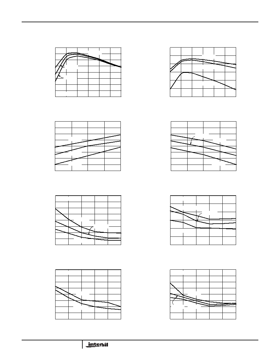
Electrical Specifications
V
DD
= V
IN
= 5V, C
OSC
= 1nF, C
SLOPE
= 470pF, T
A
= 25∞C, unless otherwise specified.
PARAMETER
DESCRIPTION
CONDITIONS
MIN
TYP
MAX
UNIT
GENERAL
I
DD
V
DD
Supply Current
OUTEN = 4V, F
OSC
= 120kHz
11
25
mA
I
DDOFF
V
DD
Standby Current
OUTEN = 0
0.1
mA
I
VIN
V
IN
No Load Current
OUTEN = 0
3
5
mA
V
OUT1
Output Initial Accuracy
VCC2DET = 4V, I
L
= 3A (see Fig. 1)
3.450
3.500
3.550
V
V
OUT2
Output Initial Accuracy
VCC2DET = 0V, I
L
= 3A, R
3
= 150
, R
4
=
100
(see Fig. 1)
2.450
2.500
2.550
V
V
OUTLINE
Output Line Regulation
V
DD
= 5V, ±10%
-1
1
%
V
OUTLOAD
Output Load Regulation
0A < I
LOAD
< 6A, relative to I
L
= 3A,
continuous mode of operation (see Fig.1)
-1
1
%
R
SHORT
Short Circuit Load Resistance
IL = 6A, prior to continuous application of
R
SHORT
, OUTEN connected to OT
100
m
I
I MAX
Current Limit
9
A
V
OUTTC
Output Tempco
-40∞C < T
A
< 85∞C
±1
%
T
OT
Over-temperature Threshold
135
∞C
T
HYS
Over-temperature Hysteresis
40
∞C
V
PWRGD
Power Good Threshold Relative to
Programmed Output Voltage
VCC2SEL = 4V, V
OUT
= 3.50V
±6
±10
±14
%
V
DDOFF
Minimum V
DD
for Shutdown
3.15
V
V
DDON
Maximum V
DD
for Startup
4.15
V
V
HYS
Input Hysteresis
V
HYS
= V
DDON
- V
DDOFF
0.5
V
M
SS
Soft-start Slope
7
V/ms
D
MAX
Maximum Duty Cycle
96
%
CONTROLLER - INPUTS
I
PUP
VCC2DET, OUTEN Pull-up Current
VCC2DET, OUTEN = 0
10
14
18
µA
I
CSLOPE
C
SLOPE
Charging Current
23
28.5
34
µA
IFB1
FB1 Input Pull-up Current
2
µA
R
OT
Over-temperature Pull-up Resistance
OT = 0V
30
40
50
k
V
IH
VCC2DET, OUTEN Input High
4
V
V
IL
VCC2DET, OUTEN Input Low
0.8
V
V
OH
PWGD
Powergood Drive High
I
LOAD
= 1mA
3.5
V
V
OL PWGD
Powergood Drive Low
I
LOAD
= -1mA
1.0
V
CONTROLLER - REFERENCE
V
REF
Reference Accuracy
I
REF
= 0
1.247
1.260
1.273
V
EL7556D
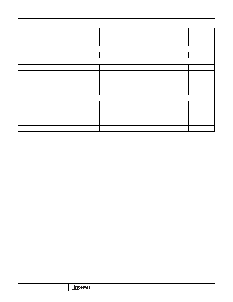
4
V
REFTC
Reference Voltage Tempco
50
ppm/∞C
V
REFLOAD
Reference Load Regulation
0 < I
LOAD
< 100µA
0.5
0.5
%/∞C
CONTROLLER - DOUBLER
VC2V
Voltage Doubler Output
V
DD
= 5V, I
LOAD
= 10mA
7.5
8.1
8.7
V
CONTROLLER - OSCILLATOR
F
RAMP
Oscillator Ramp Amplitude
1.2
V
I
OSC CHG
Oscillator Charge Current
0.2V < V
OSC
< 1.4V
150
µA
I
OSC DIS
Oscillator Discharge Current
0.2V < V
OSC
< 1.4V
5
mA
F
OSC
Oscillator Initial Accuracy
105
125
145
kHz
t
SYNC
Minimum Oscillator Sync Width
50
ns
POWER - FET
I
LEAK
L
X
Output Leakage to V
SS
L
X
= 0V
100
µA
R
DSON
Composite FET Resistance
18
30
m
R
DSONTC
R
DSON
Tempco
0.1
m
/∞C
t
BRM
FET Break Before Make Delay
10
ns
t
LEB
High Side FET Minimum on Time (LEB)
140
ns
Electrical Specifications
V
DD
= V
IN
= 5V, C
OSC
= 1nF, C
SLOPE
= 470pF, T
A
= 25∞C, unless otherwise specified.
(Continued)
PARAMETER
DESCRIPTION
CONDITIONS
MIN
TYP
MAX
UNIT
EL7556D